Chip internal structure analysis method and sample bearing device

A technology of a sample carrying device and an analysis method is applied in the field of an internal structure analysis method of a chip and a sample carrying device, and can solve the problems of low accuracy of quantitative analysis and high difficulty in sample preparation

Inactive Publication Date: 2020-10-23
YANGTZE MEMORY TECH CO LTD
View PDF9 Cites 1 Cited by
  • Summary
  • Abstract
  • Description
  • Claims
  • Application Information

AI Technical Summary

Problems solved by technology

[0003] However, the existing analysis methods have the problems of l...

Method used


Image

  • Chip internal structure analysis method and sample bearing device
  • Chip internal structure analysis method and sample bearing device
  • Chip internal structure analysis method and sample bearing device

Examples


Embodiment Construction

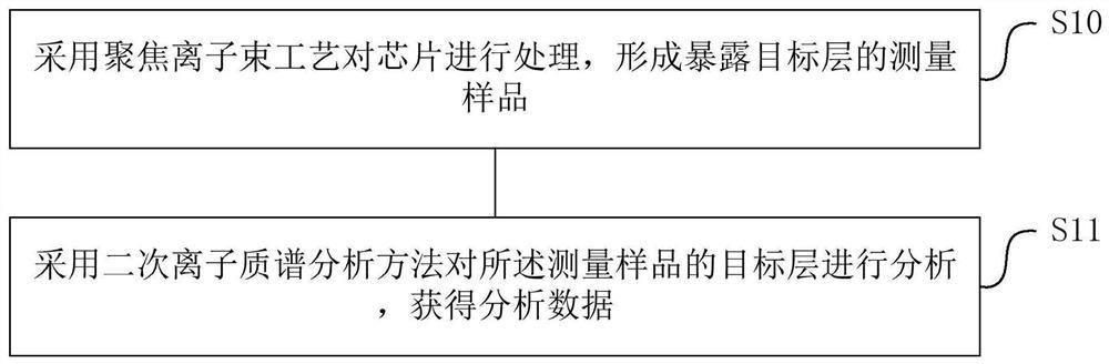
[0029] The specific implementations of the method for analyzing the internal structure of the chip and the sample carrying device provided by the present invention will be described in detail below in conjunction with the accompanying drawings.

[0030] As mentioned in the background art, the existing methods for analyzing the internal structure of chips have the problems of low quantitative analysis accuracy and high difficulty in sample preparation. Existing measurement and analysis methods include:

[0031] The disadvantage of using a test instrument with low resolution for measurement is that the accuracy of quantitative measurement is not high. The inventors found that the reason for the low accuracy is that when measuring an element with a low doping concentration, other elements as noise will affect the determination of the content of the element, thereby affecting the measurement accuracy of the element.

[0032] The disadvantage of measuring with a high-resolution te...


PUM


Abstract

The invention provides a chip internal structure analysis method and a sample bearing device. The analysis method comprises the following steps of employing the focused ion beam technology to processa chip, and forming a measurement sample exposing a target layer; and analyzing the target layer of the measurement sample by adopting a secondary ion mass spectrometry analysis method to obtain analysis data. The chip internal structure analysis method is advantaged in that the chip internal structure analysis method can be used for preparing the measurement sample with the size suitable for thechip internal structure analysis method according to the requirements of subsequent measurement and analysis steps, a target layer cannot be damaged before analysis, the sample preparation method is simple, ample preparation difficulty is reduced, the chip internal structure analysis method can be suitable for samples with most structures, meanwhile, the target layer of the prepared measurement sample is exposed on the surface of the measurement sample, so in the measurement and analysis steps, high-energy primary ion beams can directly act on the target layer, measurement accuracy is greatlyimproved, the noise influence of an additional structural layer is avoided, and precision of quantitative analysis of elements with relatively low doping concentration is greatly improved.

Description

technical field [0001] The invention relates to the field of integrated circuit manufacturing, in particular to a chip internal structure analysis method and a sample carrying device. Background technique [0002] Inside the chip, there are some specific planar structures that have specific functions, for example, use a polysilicon (poly) layer as a conductive layer, or use an oxide (oxide) layer as an isolation layer. With the improvement of the electrical requirements of the chip, the requirements for its manufacturing process are also getting higher and higher. Usually, the composition and doping (Doping) analysis of the planar structure inside the chip can be used to help improve the process technology. [0003] However, the existing analysis methods have the problems of low quantitative analysis accuracy and high difficulty in sample preparation. Therefore, there is an urgent need for a new chip internal structure analysis method to solve the above problems. Content...

Claims


Application Information

Patent Timeline
IPC IPC(8): G01N23/2258G01N23/2204G01N23/20091G01N23/00
CPCG01N23/00G01N23/20091G01N23/2204G01N23/2258
Inventor 郭起玲李亨特张顺勇刘秋艳
Owner YANGTZE MEMORY TECH CO LTD
Why Eureka
Try Eureka