Display panel, manufacturing method thereof and electronic equipment

A technology of display panel and manufacturing method, which is applied in semiconductor/solid-state device manufacturing, circuits, electrical components, etc., to achieve the effect of ensuring that signals do not interfere with each other and avoiding short-circuit problems

Pending Publication Date: 2020-10-30
CHENGDU VISTAR OPTEOLECTRONICS CO LTD
View PDF0 Cites 2 Cited by
  • Summary
  • Abstract
  • Description
  • Claims
  • Application Information

AI Technical Summary

Problems solved by technology

[0004] However, the current display panels based on

Method used


Image

  • Display panel, manufacturing method thereof and electronic equipment
  • Display panel, manufacturing method thereof and electronic equipment
  • Display panel, manufacturing method thereof and electronic equipment

Examples


Embodiment Construction

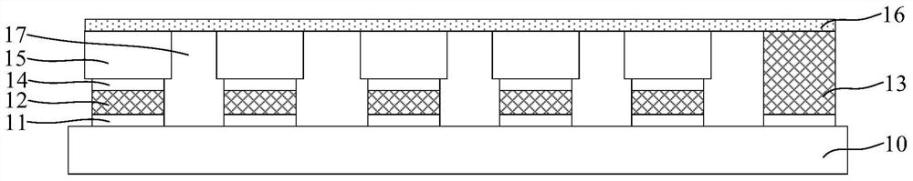
[0028] At present, the development of Micro-LED display panels based on vertical LED chips still has great technological difficulties. figure 1 It is a schematic cross-sectional structure diagram of a Micro-LED display panel, refer to figure 1 , the display panel includes: a driving backplane 10; a plurality of discrete array electrodes 11 positioned on the driving backplane 10; an LED chip, the LED chip including a lower electrode 14, an upper electrode, and a functional layer between the lower electrode 14 and the upper electrode 15, the lower electrode 14 is electrically connected to the array electrode 11 through the welding post 12; the common electrode post 13 located on the top surface of one of the array electrodes 11; a part of the common electrode layer 16 is used as the upper electrode, and the common electrode layer 16 also covers the common electrode post 13 top surface.

[0029] Wherein, the common electrode layer 16 needs to completely cover all the LED chips o...


PUM


Abstract

The invention provides a display panel, a manufacturing method thereof and electronic equipment. The manufacturing method comprises the steps of providing a driving backboard, wherein the driving backboard is provided with a plurality of discrete array electrodes; forming a spacing part on the driving backboard, a plurality of openings penetrating through the spacing part are formed in the spacingpart, and the array electrodes are exposed out of the openings; providing a plurality of light-emitting chips, wherein each light-emitting chip comprises a lower electrode and a functional layer located on the lower electrode; fixing a light-emitting chips on the array electrodes, wherein the array electrodes are electrically connected with the lower electrodes; and forming a common electrode layer, wherein the common electrode layer covers the top surfaces of the plurality of light-emitting chips and the top surface of the spacing part and is electrically connected with the functional layer.According to the invention, the common electrode layer with the whole continuous complete film layer can be formed, so that the quality of the display panel is improved.

Description

technical field [0001] Embodiments of the present invention relate to the field of display technology, and in particular to a display panel, a manufacturing method thereof, and an electronic device. Background technique [0002] With the advancement of light emitting diode (LED, Light Emitting Diode) chip technology, LED display technology using LED as light-emitting pixels becomes possible, among which Micro-LED is one of the commonly used devices in LED display technology . [0003] At present, the development of micro-light-emitting diode display panels is mostly based on flip-chip LED chip technology. In flip-chip LED chip technology, P-type electrodes and N-type electrodes (hereinafter referred to as P / N electrodes) are on the same side of the LED chip. When the electrodes are welded to the driver backplane, there are high requirements for welding accuracy and avoiding short circuits, and the corresponding welding is difficult; and the chip size of the flip-chip LED ch...

Claims


Application Information

Patent Timeline
IPC IPC(8): H01L27/12H01L33/48H01L21/84H01L25/13
CPCH01L25/13H01L33/483H01L27/1218H01L27/1262H01L2933/0033
Inventor 姚志博樊腾郭恩卿李之升
Owner CHENGDU VISTAR OPTEOLECTRONICS CO LTD
Why Eureka
Try Eureka