High-power chip routing and packaging device
A packaging device and chip bonding technology, which is applied in the direction of electrical components, semiconductor/solid-state device manufacturing, circuits, etc., can solve the problems of reducing the production efficiency of enterprises, inconvenient normal production of enterprises, and slow cooling speed, so as to improve practicability, cooling The effect of fast speed and accelerated air velocity
- Summary
- Abstract
- Description
- Claims
- Application Information
AI Technical Summary
Problems solved by technology
Method used
Image

Examples
Embodiment 1
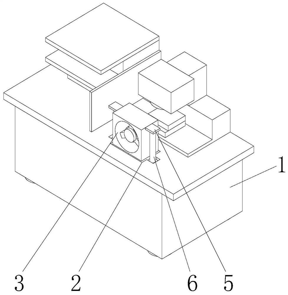
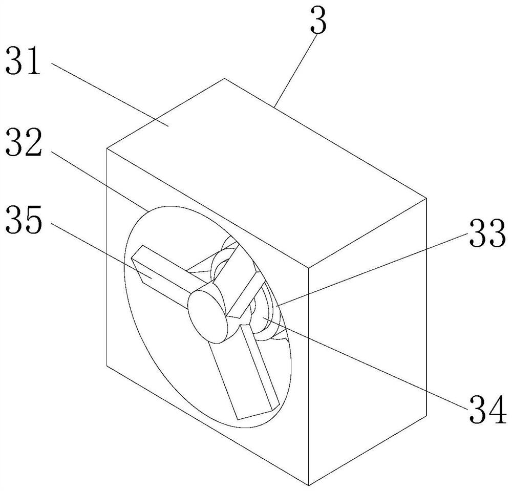
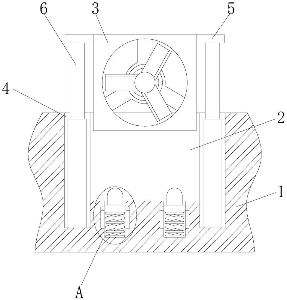
[0025] Embodiment 1: A high-power chip wire bonding packaging device, including a packaging device body 1, the four corners of the bottom of the packaging device body 1 are fixedly connected with anti-slip pads, and the bottom of the anti-slip pad is provided with anti-skid lines, through which the four corners of the bottom of the packaging device body 1 The setting of the anti-skid pad improves the stability of the packaging device body 1. The top of the packaging device body 1 is provided with a cavity 2, and the inner cavity of the cavity 2 is provided with an air-cooling structure 3. The air-cooling structure 3 includes a The mounting bracket 31 of the inner cavity, the front surface of the mounting bracket 31 is provided with a mounting hole 32, the inner cavity of the mounting hole 32 is fixedly connected with a fixed frame 33, and the inner cavity of the fixed frame 33 is fixedly connected with a motor 34, and the output shaft of the motor 34 is fixed. The fan blade 35 ...
Embodiment 2
[0026]Embodiment 2: A high-power chip wire bonding packaging device, including a packaging device body 1, the four corners of the bottom of the packaging device body 1 are fixedly connected with anti-slip pads, the bottom of the anti-slip pad is provided with anti-slip lines, and the top of the packaging device body 1 is opened There is a cavity 2, the inner cavity of the cavity 2 is provided with an air-cooling structure 3, the air-cooling structure 3 includes a mounting frame 31 located in the cavity of the cavity 2, and the front surface of the mounting frame 31 is provided with a mounting hole 32, and the mounting hole 32 The inner chamber of the fixed mount 33 is fixedly connected with a fixed frame 33, the inner cavity of the fixed frame 33 is fixedly connected with a motor 34, and the output shaft of the motor 34 is fixedly connected with a fan blade 35, through the mounting frame 31, the mounting hole 32, the fixed frame 33, the motor 34 and The cooperative use of the f...
Embodiment 3
[0027] Embodiment 3: A high-power chip wire bonding packaging device, including a packaging device body 1, the four corners of the bottom of the packaging device body 1 are fixedly connected with anti-slip pads, and the bottom of the anti-slip pad is provided with anti-skid lines, through which the four corners of the bottom of the packaging device body 1 The setting of the anti-skid pad improves the stability of the packaging device body 1. The top of the packaging device body 1 is provided with a cavity 2, and the inner cavity of the cavity 2 is provided with an air-cooling structure 3. The air-cooling structure 3 includes a The mounting bracket 31 of the inner cavity, the front surface of the mounting bracket 31 is provided with a mounting hole 32, the inner cavity of the mounting hole 32 is fixedly connected with a fixed frame 33, and the inner cavity of the fixed frame 33 is fixedly connected with a motor 34, and the output shaft of the motor 34 is fixed. The fan blade 35 ...
PUM
 Abstract
Description
Claims
Application Information
 - R&D
- Intellectual Property
- Life Sciences
- Materials
- Tech Scout
- Unparalleled Data Quality
- Higher Quality Content
- 60% Fewer Hallucinations
Browse by: Latest US Patents, China's latest patents, Technical Efficacy Thesaurus, Application Domain, Technology Topic, Popular Technical Reports.
© 2025 PatSnap. All rights reserved.Legal|Privacy policy|Modern Slavery Act Transparency Statement|Sitemap|About US| Contact US: help@patsnap.com