Rotary pre-correction device for silicon wafer

A pre-correction and silicon wafer technology, which is applied to the exposure device of photolithography process, transportation and packaging, photoplate process of pattern surface, etc., can solve the problems of lithography machine stop alarm, affect work efficiency, inconsistency, etc., and achieve improvement Accuracy, simple structure, good correction effect

Pending Publication Date: 2020-11-06
江苏晋誉达半导体股份有限公司
View PDF0 Cites 0 Cited by
  • Summary
  • Abstract
  • Description
  • Claims
  • Application Information

AI Technical Summary

Problems solved by technology

[0003] However, there will be a problem during the working process. Although the position of the flower basket can be accurately positioned, the position of the silicon chip in the flower basket is not consistent. Generally, the silicon chip is placed in the slot of the flower basket, and the left and right sides of the flower basket The side wall is adapted to the diameter of the silicon wafer. One end of the flower basket is open and the other end has an end wall. After the silicon wafer is inserted into the slot, the silicon wafer may not be in full contact with the end wall, especially when the flower basket is moved to During the process of placing the platform, the position of the silicon wafer may also change such as shaking. Therefore, even if the silicon wafer is originally placed relatively accurately, the position of the silicon wafer will still change during the moving process. When the silicon wafer is transferred to the lithography area, the position of the silicon wafer will shift. Then, when the position deviation is relatively large, the edge-seeking action cannot be completed, causing the lithography machine to stop and alarm, which seriously affects the work efficiency.

Method used


Image

  • Rotary pre-correction device for silicon wafer
  • Rotary pre-correction device for silicon wafer
  • Rotary pre-correction device for silicon wafer

Examples


Embodiment Construction

[0035] The present invention will be described in further detail below through specific examples.

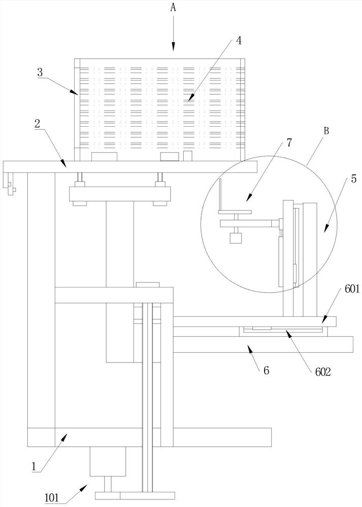
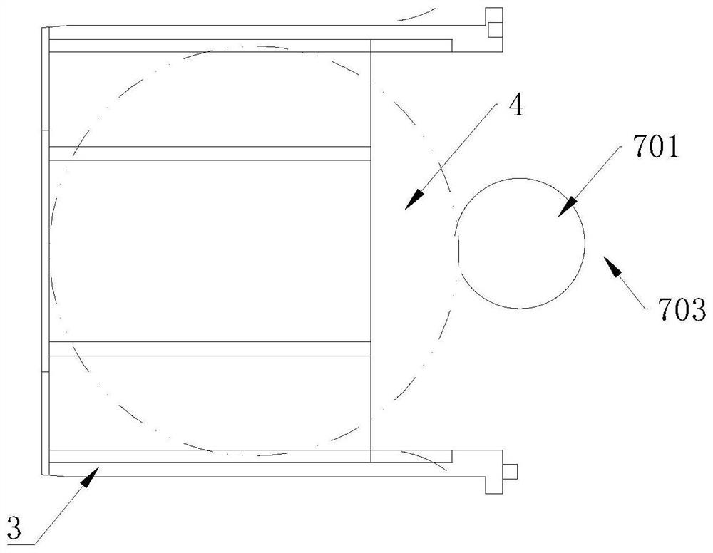
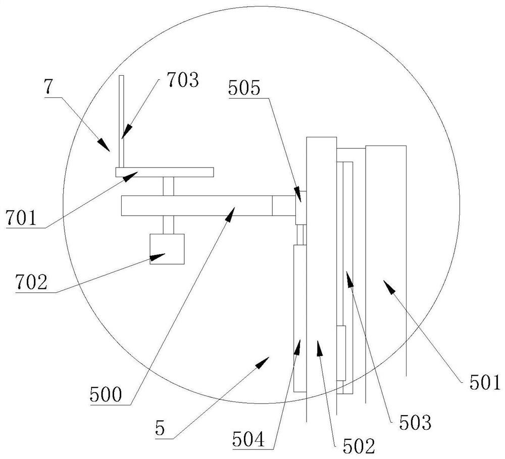
[0036] Such as figure 1 As shown, a rotating pre-correction device for silicon wafers includes a frame 1, and the frame 1 is provided with a placement platform 2 driven by a lifting drive device 101 (a lifting drive component such as a cylinder), and a silicon wafer is positioned on the placement platform 2. Chip holding box 3 (preventing many silicon wafers 4 in it), this frame 1 is also provided with horizontal support 6, and this horizontal support 6 is provided with vertical driving mechanism 5, drives on this vertical driving mechanism 5 There is a support base 500, on which a correcting mechanism 7 is rotatably installed, and the correcting mechanism 7 is arranged on the same side as the opening end of the silicon wafer storage box 3 (see figure 2 ).

[0037] The correction mechanism 7 includes a turntable 701 that is rotatably installed on the support base 500 and arra...


PUM


Abstract

The invention discloses a rotary pre-correction device for a silicon wafer. The device comprises a machine frame, a placing platform driven by a lifting driving device is arranged on the machine frame, a silicon wafer containing box is positioned on the placing platform, a horizontal support is arranged on the machine frame, a vertical driving mechanism is arranged on the horizontal support, a supporting base is driven by the vertical driving mechanism, a correcting mechanism is installed on the supporting base in a rotating mode, and the correcting mechanism and the opening end of the siliconwafer containing box are arranged on the same side. The supporting base is driven by the vertical driving mechanism to ascend and get close to the silicon wafer in the silicon wafer containing box; then force is applied to the silicon wafer through the rotating correcting mechanism, and the silicon wafer abuts against the end arm on the silicon wafer containing box, so that before the silicon wafer is transferred to the photoetching machine, the reset correction work of the silicon wafer (the position of the silicon wafer is changed) is completed, the accuracy of transferring the silicon wafer to a photoetching area is improved, and the continuity and the working efficiency of normal working of the photoetching machine are effectively guaranteed.

Description

technical field [0001] The invention belongs to the technical field of silicon wafer rectification, and in particular relates to a silicon wafer rotation pre-alignment device. Background technique [0002] A photolithography machine is a commonly used equipment in the semiconductor production process. Its working process is: place a silicon wafer holding box (generally called a flower basket) containing several silicon wafers on a liftable placement platform , the placement platform is equipped with a positioning structure to accurately position the position of the flower basket, and then use the pick-up mechanism to take out the silicon wafers in the flower basket one by one and send them to the lithography station of the lithography machine. Edge finding is performed to finally determine the edge position of the silicon wafer and determine the photolithography area. [0003] However, there will be a problem during the working process. Although the position of the flower b...

Claims


Application Information

Patent Timeline
Patent Type & Authority Applications(China)
IPC IPC(8): G03F7/20B65G47/22B65G47/82
CPCB65G47/22B65G47/82G03F7/7075G03F7/70775
Inventor 黄佳
Owner 江苏晋誉达半导体股份有限公司
Why Eureka
Try Eureka