Image processing method and device based on semiconductor defect detection, equipment and medium

A defect detection and image processing technology, which is applied in the field of data processing, can solve problems such as time-consuming ultrasonic technology, damage to the chip circuit structure by X-rays, and inability to penetrate the chip.

Inactive Publication Date: 2020-11-20
JIHUA LAB
View PDF5 Cites 7 Cited by
  • Summary
  • Abstract
  • Description
  • Claims
  • Application Information

AI Technical Summary

Problems solved by technology

Optical inspection cannot see inside the semiconductor because it cannot penetrate the chip's packaging material and PCB board
Due to the use of acoustic couplants during testing, ultrasonic techniques are time consuming and fouling, and can only be performed on a sample basis
X-ray technology can only detect metals, not cracks, delaminations or holes in the non-metallic ground inside the chip
In addition, the ionization characteristics of X-rays may damage the internal circuit structure of the chip and cause personal injury to the on-site workers

Method used


Image

  • Image processing method and device based on semiconductor defect detection, equipment and medium
  • Image processing method and device based on semiconductor defect detection, equipment and medium
  • Image processing method and device based on semiconductor defect detection, equipment and medium

Examples


Embodiment Construction

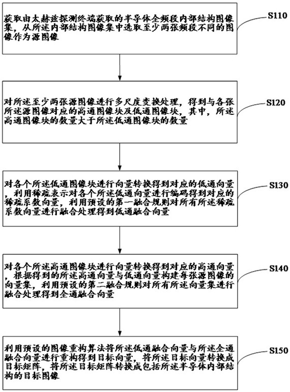
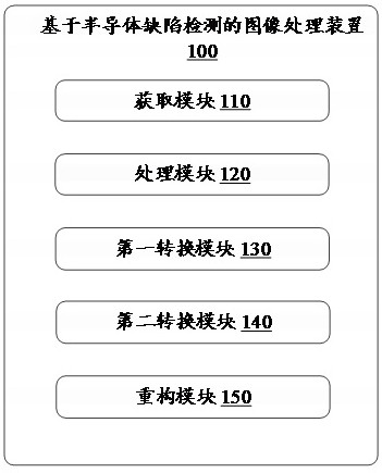
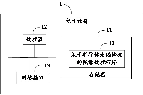
[0040] In order to make the purpose, technical embodiment and advantages of the present invention clearer, the present invention will be further described in detail below in conjunction with the accompanying drawings and embodiments. It should be understood that the specific embodiments described here are only used to explain the present invention, not to limit the present invention. Based on the embodiments of the present invention, all other embodiments obtained by persons of ordinary skill in the art without making creative efforts belong to the protection scope of the present invention.

[0041]It should be noted that the descriptions involving "first", "second", etc. in the present invention are only for descriptive purposes, and should not be understood as indicating or implying their relative importance or implicitly indicating the number of indicated technical features . Thus, the features defined as "first" and "second" may explicitly or implicitly include at least o...


PUM


Abstract

The invention relates to the field of data processing, and provides an image processing method and device based on semiconductor defect detection, equipment and a medium. The method comprises the steps: acquiring a semiconductor full-band internal structure image set, and selecting images with different frequency bands from the internal structure image set to serve as source images; processing thesource image to obtain a high-pass image block and a low-pass image block, converting the low-pass image block to obtain a low-pass vector, encoding the low-pass vector to obtain corresponding sparsecoefficient vectors, and performing fusion processing on all the sparse coefficient vectors to obtain a low-pass fusion vector; converting the high-pass image block to obtain a high-pass vector, constructing a vector set of each source image according to the high-pass vector and the low-pass vector, and performing fusion processing on all the vector sets to obtain an all-pass fusion vector; reconstructing the low-pass fusion vector and the all-pass fusion vector to obtain a target vector, and converting the target vector into a target image. The definition of semiconductor imaging can be improved, and therefore the semiconductor defect detection precision is improved.

Description

technical field [0001] The present invention relates to the field of data processing, in particular to an image processing method, device, equipment and medium based on semiconductor defect detection. Background technique [0002] The defect detection of semiconductor chips is an important step in the process of manufacturing semiconductor chips, and the decision is the yield rate of semiconductor chips. The main ways of semiconductor chip defects are uneven internal structure of the wafer, peeling of the internal circuit of the chip, breakage of chip packaging leads, and stress failure of packaging materials. [0003] At present, the commonly used semiconductor defect detection technologies in the industry are optical detection, ultrasonic detection, and X-ray detection, but these technologies have certain limitations. Optical inspection cannot see inside the semiconductor because it cannot penetrate the chip's packaging material and PCB board. Due to the use of acoustic ...

Claims


Application Information

Patent Timeline
Patent Type & Authority Applications(China)
IPC IPC(8): G06T7/00G06T5/50G06T5/10G06T5/00G06F17/16
CPCG06F17/16G06T5/002G06T5/10G06T5/50G06T7/0004G06T2207/20016G06T2207/30141G06T2207/30148
Inventor 毛淇刘竞博吕赐兴朱云龙
Owner JIHUA LAB
Why Eureka
Try Eureka