Grain processing device for semiconductor graphite wafer and operation method thereof

A processing device and semiconductor technology, which is used in the manufacture of semiconductor/solid state devices, machine tools suitable for grinding workpiece planes, grinding drive devices, etc. The problems such as the complex fixing method of the circle can reduce labor intensity, improve grinding efficiency, and increase the scope of clamping use.

Inactive Publication Date: 2020-11-24
DATONG XINCHENG NEW MATERIAL CO LTD
View PDF8 Cites 10 Cited by
  • Summary
  • Abstract
  • Description
  • Claims
  • Application Information

AI Technical Summary

Problems solved by technology

[0002] Wafer finishing equipment is used to polish wafers and grains to improve the smoothness of the wafer surface. In traditional wafer finishing, it is not convenient to process wafers of different sizes due to the complicated way of fixing the wafers. The plate is clamped, and at the same time, it is easy to cause damage to the wafer plate during clamping; when the grains on the wafer plate are polished, the method of manual grinding operation is often used, which is easy to cause when the grains are polished, due to The long-time grinding operation greatly reduces the physical strength and energy of the staff, which affects the quality of the grain grinding on the wafer board and is not convenient for the staff to perform the grinding operation

Method used


Image

  • Grain processing device for semiconductor graphite wafer and operation method thereof
  • Grain processing device for semiconductor graphite wafer and operation method thereof
  • Grain processing device for semiconductor graphite wafer and operation method thereof

Examples


Embodiment 1

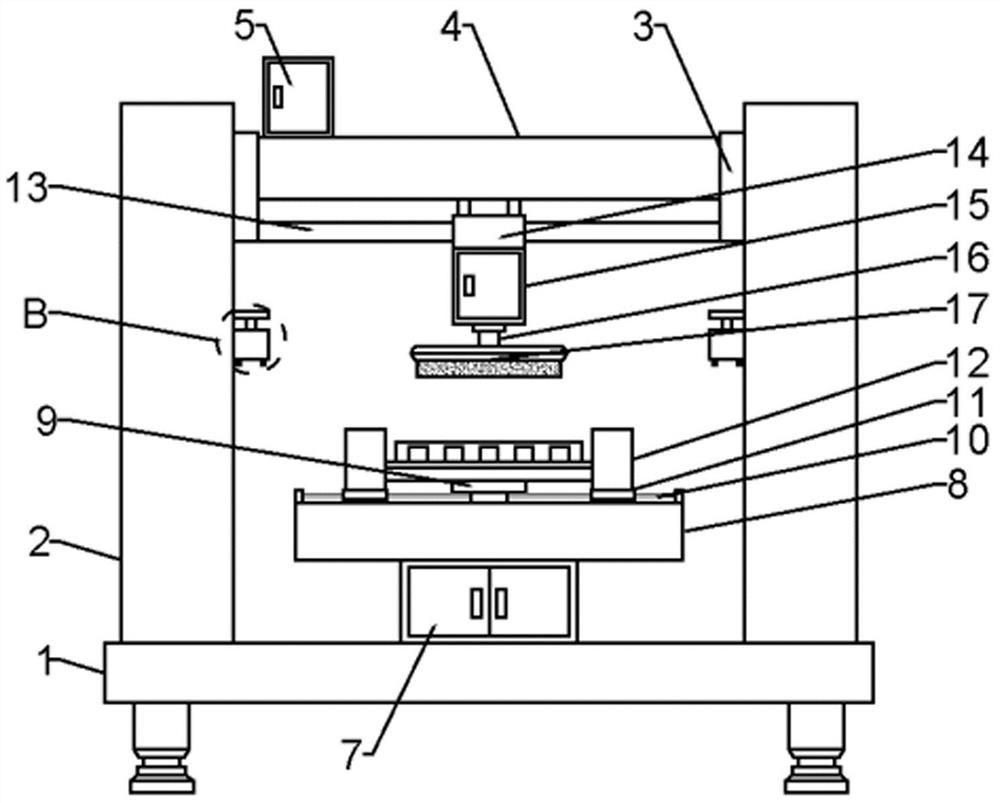
[0030] Example 1: see Figure 1-4 , a grain processing device for semiconductor graphite wafers, comprising a base 1, a column 2 is vertically fixed in the middle of both sides of the top surface of the base 1, and a column 2 is vertically fixed on the upper parts of the inner sides of the two columns 2. Be provided with movable plate 3 to the activity, be provided with crossbeam 4 horizontally on the top between two described movable plates 3, be fixedly provided with motor box 5 in the middle part of one end of the top surface of described crossbeam 4, in described motor box 5 The first motor 6 is vertically fixed inside, and the model of the first motor 6 is T63B4; a rectangular equipment box 7 is fixedly installed in the middle of the top surface of the base 1, and a horizontally fixed equipment box 7 is installed on the top surface of the equipment box 7. There is a rectangular bearing platform 8, a rectangular fixing block is fixed in the middle of the top surface of the...

Embodiment 2

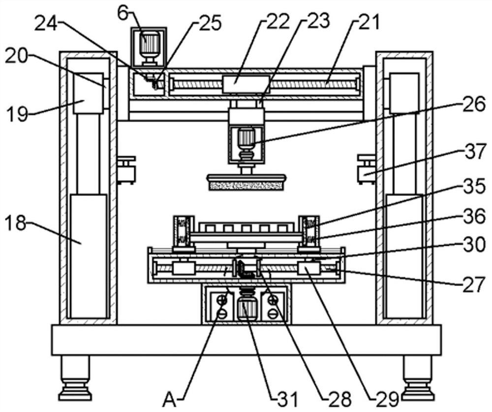
[0036] Example 2: see Figure 5 , in the present embodiment, the present invention also proposes a method for operating a grain processing device for a semiconductor graphite wafer, comprising the following steps:

[0037] Step 1, at first the first motor 6, the electric push cylinder 18, the second motor 26 and the third motor 31 are respectively electrically connected to the storage battery through wires, and the wafer plate is placed on the top surface of the rubber pallet 9, and then according to The size of the wafer plate is adjusted to the distance between the curved splints on both sides;

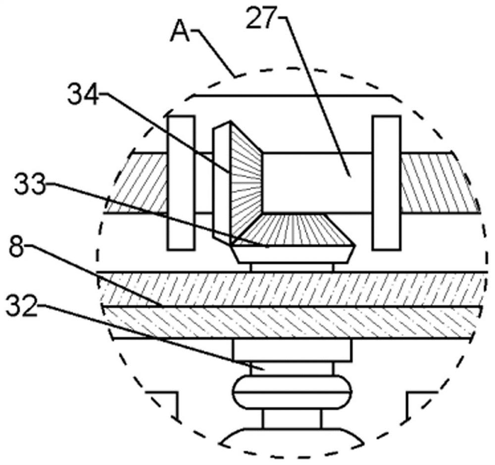
[0038] Step 2, drive the driving bevel gear 33 at the top of the drive shaft 32 to rotate by controlling the third motor 31, drive the rotating rod 27 to rotate through the meshing transmission of the driving bevel gear 33 and the driven bevel gear 34, and rotate through the driving bevel gear 33 on the rod body of the rotating rod 27. The forward thread and the reverse thread driv...


PUM


Abstract

The invention discloses a grain processing device for a semiconductor graphite wafer. The device includes a base, stand columns are arranged in the middles of two sides of the top face of the base, anequipment tank is arranged on the top face of the base, a bearing table is arranged on the top face of the equipment tank, a rubber carrying plate is arranged at the top end of a fixing block, T-shaped guide rails are arranged on the top face of the bearing table on two sides of the fixing block, an arc-shaped clamp plate is arranged on the top face of each sliding plate, wafer plates are placedon the top face of the rubber carrying plate, a driving tank is arranged at the bottom of a sleeve pipe, a rotating shaft is arranged on the inner bottom face of the driving tank, and a grinding wheelsleeves the bottom end of the rotating shaft. The device is convenient to operate, through a driving assembly and an adjusting assembly, the problems that the wafer plates are prone to damaging during clamping, the wafer plates with different size are not convenient to clamp and the clamping efficiency is comparatively low can be solved, and through a moving assembly and a lifting assembly, the problem that the operation is not convenient when an existing grain grinding device grinds grains on the wafer plates can be solved.

Description

technical field [0001] The invention relates to the technical field of semiconductor graphite wafer processing, in particular to a grain processing device for semiconductor graphite wafers and an operating method thereof. Background technique [0002] Wafer finishing equipment is used to polish wafers and grains to improve the smoothness of the wafer surface. In traditional wafer finishing, it is not convenient to process wafers of different sizes due to the complicated way of fixing the wafers. The plate is clamped, and at the same time, it is easy to cause damage to the wafer plate during clamping; when the grains on the wafer plate are polished, the method of manual grinding operation is often used, which is easy to cause when the grains are polished, due to The long-time grinding operation greatly reduces the physical strength and energy of the staff, which affects the quality of the grain grinding on the wafer plate and is not convenient for the staff to perform the gri...

Claims


Application Information

Patent Timeline
IPC IPC(8): B24B7/22B24B27/00B24B41/00B24B41/06B24B41/02B24B47/12B24B47/04H01L21/67
CPCB24B7/228B24B27/0046B24B41/007B24B41/02B24B41/068B24B47/04B24B47/12H01L21/67092
Inventor 柴万红张培林武建军柴利春张作文王志辉
Owner DATONG XINCHENG NEW MATERIAL CO LTD
Why Eureka
Try Eureka