Magnetic domain wall writing unit and method based on multiferroic heterostructure

A technology of heterogeneous structure and writing unit, applied in information storage, static memory, digital memory information and other directions, can solve the problems of low storage density, high Joule heat, large memory unit volume, etc., to increase storage density, reduce Unit volume, solving the effect of large memory unit volume

Active Publication Date: 2020-11-27
CHINA JILIANG UNIV
View PDF7 Cites 0 Cited by
  • Summary
  • Abstract
  • Description
  • Claims
  • Application Information

AI Technical Summary

Problems solved by technology

[0004] Aiming at the problems of large volume of memory cells, low storage density and high Joule heat when magnetic domain walls are written into track memory in the prior art, the present invention provides a magnetic domain wall writing method based on a multiferroic heterostructure The unit and method utilize the inverse piezoelectric effect and the inverse effect of magnetostriction, by applying a voltage to the piezoelectric layer on the top electrode and the bottom electrode layer, an electric field is generated in the piezoelectric layer so that the piezoelectric layer is strained and transmitted to the magnetic layer, and then affect the magnetic anisotropy of the magnetic material, so that the magnetization direction of the magnetic material in the electrode layer area changes, thereby inducing the magnetic domain wall, which has the characteristics of small volume, high storage density and less heat generation

Method used


Image

  • Magnetic domain wall writing unit and method based on multiferroic heterostructure
  • Magnetic domain wall writing unit and method based on multiferroic heterostructure
  • Magnetic domain wall writing unit and method based on multiferroic heterostructure

Examples


Embodiment 1

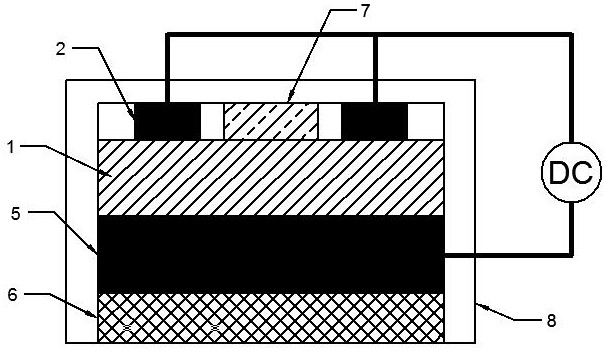
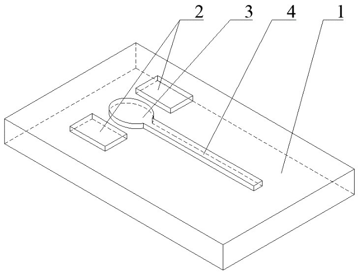
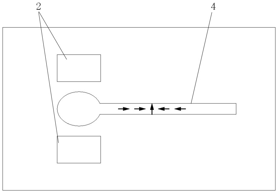
[0022] like figure 1 As shown, it is a magnetic domain wall writing unit based on a multiferroic heterostructure, including: a bottom electrode layer 5, connected to a pulse voltage source; a piezoelectric layer 1, made of a ferroelectric material, disposed on the bottom electrode layer 5 Top; 2 layers of top electrodes, set on the piezoelectric layer 1, including two top electrodes 2 connected to the pulse voltage source; magnetic layer 7, on the same layer as the top electrodes 2, made of ferromagnetic material, connected to the track Memory; wherein the ferromagnetic material of the magnetic layer 7 has magnetic anisotropy and magnetostrictive properties. In the traditional way, nanowires are used to inject magnetic fields to generate domain walls, and inject spin current to generate spin transfer torque to push the magnetic domain walls. Therefore, during the entire working process of the device, current continuously flows through the wires to generate a large amount of Jo...

Embodiment 2

[0033] like Figure 4 As shown, this embodiment is generally consistent with the previous embodiment, except that the magnetic domain wall generation region 3 is rhombus-shaped.


PUM


Abstract

The invention discloses a magnetic domain wall writing unit and method based on a multiferroic heterostructure, and the unit comprises a bottom electrode layer which is connected with a pulse voltagesource; the piezoelectric layer is made of a ferroelectric material and is arranged on the bottom electrode layer; the top electrode layer is arranged on the piezoelectric layer and comprises a plurality of top electrodes connected with a pulse voltage source; the magnetic layer and the top electrode are located on the same layer, and the magnetic layer is made of ferromagnetic materials and connected with the track memory; wherein the ferromagnetic material of the magnetic layer has magnetic anisotropy and magnetostriction characteristics. Pulse voltage is applied to the top electrode layer and the bottom electrode layer to enable the piezoelectric layer to generate strain, the strain is transmitted to the magnetic layer and induced to generate a magnetic domain wall, and the magnetic domain wall is driven to the racing track memory; and adjusting the pulse voltage to change the strain degree of the piezoelectric layer so as to write different data. Magnetic domain wall writing with high storage density and low power consumption is realized by utilizing an inverse piezoelectric effect and a magnetostriction inverse effect.

Description

technical field [0001] The invention relates to the technical field of spin electronics, in particular to a magnetic domain wall writing unit and method based on a multiferroic heterostructure. Background technique [0002] As a new type of non-volatile spin information storage device, track memory has high application potential for building a future three-dimensional storage framework. The track memory stores multi-bit information on the magnetic nanostrips in the form of magnetic domains, and the multi-bit information is distinguished by magnetic domain walls, so as to achieve the purpose of high-density storage, and can also achieve fast information reading and writing. There is an electrode perpendicular to the nanostrip below the track memory as a data write line. When a pulse current is injected into the electrode, the Oersted field generated by the current can change the magnetization direction of the adjacent nanostripes, so that data can be written or modified. Al...

Claims


Application Information

Patent Timeline
IPC IPC(8): G11C11/22
CPCG11C11/2275
Inventor 邱阳施胜宾周浩淼杨浛朱明敏郁国良
Owner CHINA JILIANG UNIV
Why Eureka
Try Eureka