Digital signal glitch elimination circuit and glitch elimination method

A technology for eliminating circuits and digital signals, which is applied to logic circuits with logic functions, electrical components, pulse processing, etc. It can solve the problems of small burr width programming and large logic complex area, and achieve the effect of ensuring transmission and pick-up

Pending Publication Date: 2020-11-27
SHANGHAI CHIPANALOG MICROELECTRONICS LTD
View PDF6 Cites 1 Cited by
  • Summary
  • Abstract
  • Description
  • Claims
  • Application Information

AI Technical Summary

Problems solved by technology

However, the above two types of burr elimination circuits can only eliminate high-level or low-level burrs, and the programming degree of the width of the burr that can be eliminated is small, and has the disadvantages of complex logic and large area.

Method used


Image

  • Digital signal glitch elimination circuit and glitch elimination method
  • Digital signal glitch elimination circuit and glitch elimination method
  • Digital signal glitch elimination circuit and glitch elimination method

Examples


Embodiment 1

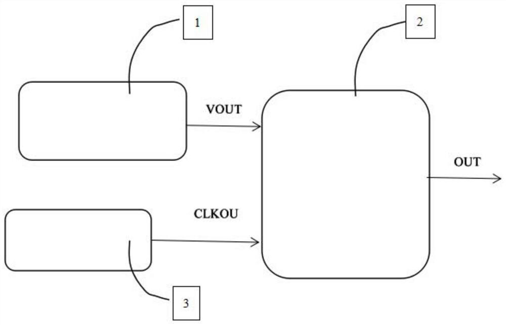
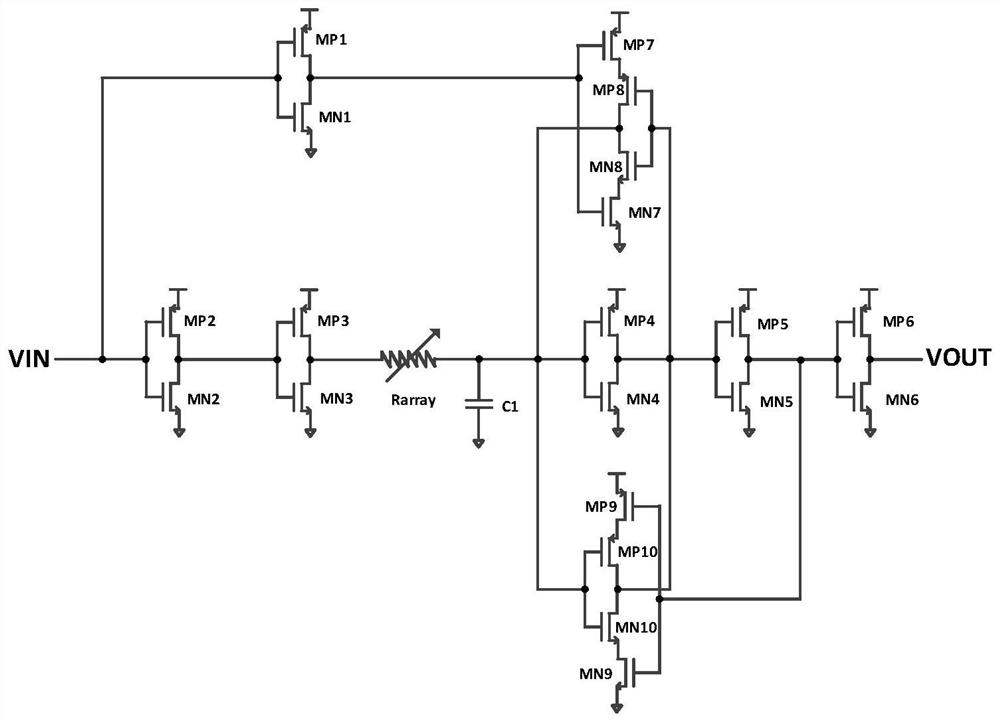
[0043] Please refer figure 1 As shown, a digital signal glitch elimination circuit. In this embodiment, the glitch elimination circuit includes an analog elimination circuit 1, and the analog elimination circuit 1 includes a MOS inverter, a MOS nested inverter, a resistor array, and a capacitor. The output end of the analog cancellation circuit 1 is electrically connected to the digital cancellation circuit 2. The digital cancellation circuit 2 is provided with a signal link unit and a logic processing unit, and the signal link unit is used to delay processing the input digital signal at different times , The logic processing unit is used to perform logic operations on digital signals with different delays.

[0044] Analog elimination circuit 1 is used to eliminate digital signal glitches whose glitch time width is less than the period of the input clock signal of the digital elimination unit and output as VOUT, and digital elimination circuit 2 is used to eliminate digital signal...

Embodiment 2

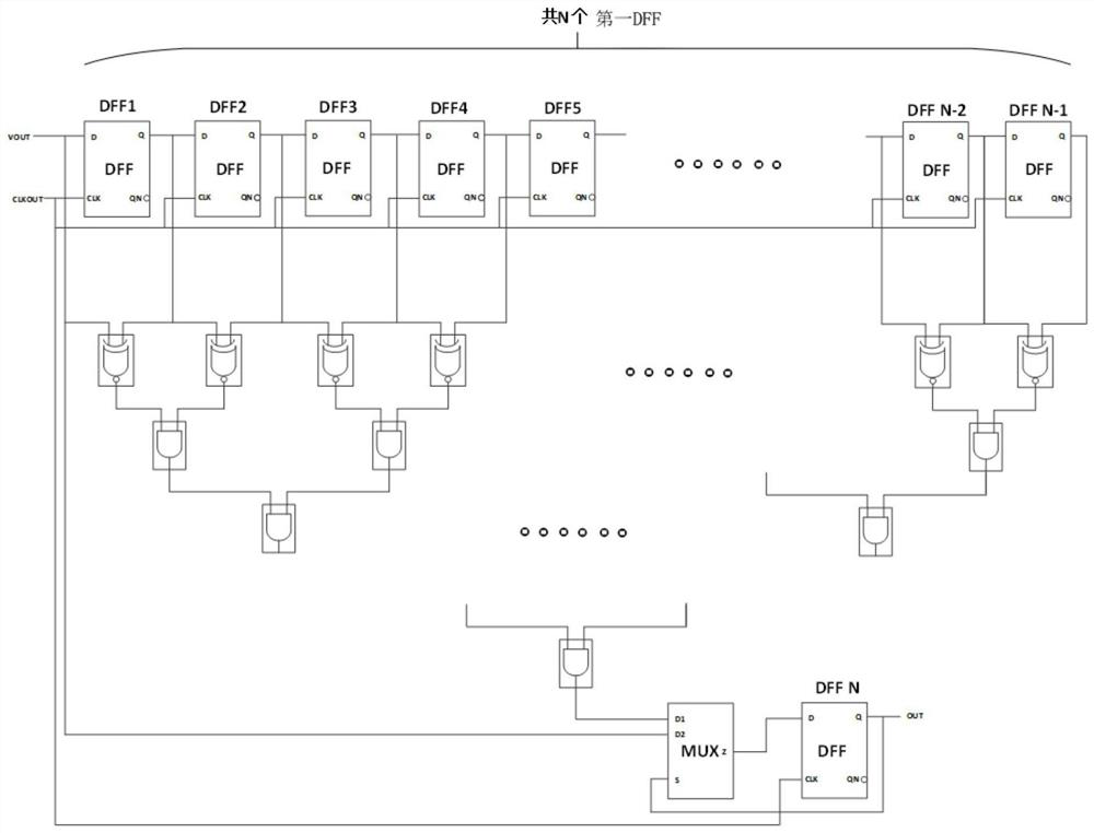
[0056] Please refer figure 1 As shown, this embodiment provides another digital signal glitch elimination circuit. The purpose of this embodiment is to add a clock divider unit 3 to the glitch elimination circuit on the basis of Embodiment 1. The clock divider unit 3 is used for The frequency of the input clock signal is divided to obtain a clock period suitable for the digital cancellation unit. Through the design of the programmable clock divider unit 3, the period of the input clock signal generated in the digital canceling circuit 2 can be adjusted, so that the glitch canceling circuit of the digital signal can be applied to various structures of digital isolators, wireless communications and other components. Elimination of burrs.

[0057] Such as figure 1 and Figure 4 As shown, the clock frequency dividing unit 3 includes M second D flip-flops connected in series, the input clock period of the second D flip-flop is tclk, and M is an integer greater than or equal to 0. In...

Embodiment 3

[0063] This embodiment provides a digital signal burr elimination method, which is applied to the burr elimination circuit of the above-mentioned embodiment 1 and embodiment 2 to eliminate the burr of the digital signal, and the clock frequency division unit 3 is electrically connected to the digital elimination circuit 2. At this time, the period of the input clock signal generated by the signal link unit and the logic processing unit is (2 M )*(N-1)*tclkin; The method of removing glitches from digital signals includes the following steps:

[0064] Step 100, the digital signal is input to the analog elimination circuit 1, and the time width of the elimination of the glitch by the analog elimination circuit 1 is less than (2 M )*(N-1)*tclkin's digital signal glitch, and output as VOUT;

[0065] Step 200: The output VOUT of the analog cancellation circuit 1 is electrically connected to the data input terminal D of the first first D flip-flop, and the output CLKOUT of the clock freque...


PUM


Abstract

The invention provides a digital signal glitch elimination circuit, which comprises an analog elimination circuit, and is characterized in that the analog elimination circuit comprises an MOS inverter, an MOS nested inverter, a resistor array and a capacitor. The output end of the analog elimination circuit is electrically connected with a digital elimination circuit, a signal link unit and a logic processing unit are arranged in the digital elimination circuit, the signal link unit is used for carrying out delay processing on an input digital signal, and the logic processing unit is used forcarrying out logic operation on the digital signal subjected to delay processing. The analog elimination circuit is used for eliminating digital signal glitches whose glitch time width is smaller thanan input clock signal period, and the digital elimination circuit is used for eliminating digital signal glitches whose glitch time width is larger than the input clock signal period and outputting the digital signal glitches as OUT. Through the combination of the analog elimination circuit and the digital elimination circuit, burrs generated in the digital signal transmission process are eliminated, and the circuit has the advantages of being capable of eliminating high-level and low-level burrs at the same time, programmable in burr elimination time width, small in area and the like.

Description

Technical field [0001] The invention belongs to the field of integrated circuit design and relates to digital signal processing technology, in particular to a digital signal burr elimination circuit and a burr elimination method. Background technique [0002] The transmission of digital signals is common in the field of integrated circuit design such as digital isolators and wireless communications. However, due to timing errors, interference signals and other factors, a large number of random glitches are often generated during the transmission of digital signals. The existence of random glitches can interfere with the transmission of digital signals, and even cause signal reception failures in severe cases. Therefore, it is usually necessary to add a glitch elimination circuit in the digital signal transmission path to eliminate the glitch and retain the complete desired signal. [0003] At present, the existing glitch elimination circuits are mainly divided into two categories:...

Claims


Application Information

Patent Timeline
Patent Type & Authority Applications(China)
IPC IPC(8): H03K5/1252H03K19/20
CPCH03K5/1252H03K19/20
Inventor 杨峰
Owner SHANGHAI CHIPANALOG MICROELECTRONICS LTD
Why Eureka
Try Eureka