Method for Determining Incident Particle Type or Action Location Based on Pulse Waveform Discrimination
A pulse waveform and type technology, applied in the field of radiation detection, can solve the problems of poor discrimination effect, noise sensitivity, and failure to obtain discrimination effect, etc., and achieve the effect of improving pulse waveform discrimination ability, strong anti-noise ability, and strong waveform discrimination ability
- Summary
- Abstract
- Description
- Claims
- Application Information
AI Technical Summary
Problems solved by technology
Method used
Image
Examples
specific Embodiment approach 1
[0046] Embodiment 1 (for particle type screening):
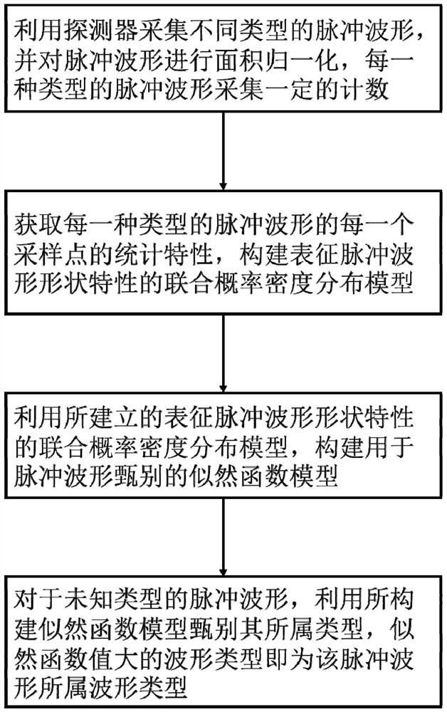
[0047] The neutron / gamma particle screening method based on full waveform statistical properties of the present invention has the following steps:
[0048] The detector used is a CLYC crystal detector, wherein the CLYC crystal size is 2.54 cm (φ)×2.54 cm (H), that is, the crystal size is a cylinder with a diameter and a height of 2.54 cm. One end of the CLYC crystal is coupled to a PMT for photoelectric signal conversion. Gamma or neutron incident CLYC crystal will interact with it to deposit energy to generate scintillation photons, which are transported to the PMT terminal, and photoelectrons are shot on the PMT photocathode to complete photoelectric conversion and output pulse waveform signals. Each neutron or gamma photon event can generate a pulse signal waveform. The PMT back-end electronics performs analog-to-digital conversion on the output pulse signal of the PMT and completes the signal waveform acquisition. Th...
specific Embodiment approach 2
[0066] Specific embodiment 2 (for ray action position extraction)
[0067] The ray action position extraction method based on full waveform statistical characteristics of the present invention has the following steps:
[0068] The detector used is "Phoswich" detector, the crystal types used are LYSO, YSO, GAGG and BGO respectively, and the luminescence decay time constants are 40ns, 60ns, 140ns and 300ns respectively. The size of the crystals is 1.5mm×1.5mm×10mm, and four kinds of crystals form a 2×2 array, in which an ESR reflective film with a thickness of about 0.1mm is pasted between the crystals, the outside and the top surface of the crystals to avoid optical crosstalk And light loss, the bottom surface of the crystal array is coupled to a silicon photomultiplier device SiPM unit, the SiPM product model used is SensL FC30035. The gamma photon incident crystal array reacts to deposit energy to generate scintillation photons, and the scintillation photons are transporte...
PUM
 Abstract
Description
Claims
Application Information


