A device with functions of crystal structure detection and in-situ repair

A technology of crystal structure and in-situ repair, applied in semiconductor/solid-state device manufacturing, electrical components, circuits, etc., can solve the problem of uneven distribution of crystal defects on the surface of large-scale semiconductor thin film materials, and the difficulty of achieving precision on the surface of large-scale semiconductor thin film materials. problems such as positioning, inability to efficiently target and repair thin-film materials, etc., to achieve the effect of small heat-affected range, improved uniformity and crystal quality, and short action time

Active Publication Date: 2021-07-20
WUHAN UNIV
View PDF6 Cites 0 Cited by
  • Summary
  • Abstract
  • Description
  • Claims
  • Application Information

AI Technical Summary

Problems solved by technology

[0003] At present, for the crystal defects of semiconductor thin film materials, the existing methods mainly focus on heat treatment of the whole thin film material or irradiating the local area of ​​the thin film material with pulsed laser. However, the distribution of crystal defects on the surface of large semiconductor thin film materials is often not uniform. The overall heat treatment cannot perform more efficient and targeted repairs on local areas according to individual differences in film materials
Although pulsed laser radiation can repair crystal defects in local areas of semiconductor thin film materials, the detection of crystal structure and the repair process of defects are often carried out separately. It is difficult to achieve precise positioning on the surface of large-size semiconductor thin film materials, and the repair process is not targeted and efficient. Efficiency
In addition, the existing overall heat treatment method is mainly low temperature, and the peak power of pulsed laser radiation treatment is relatively low, so for diamond, gallium nitride, silicon carbide, aluminum nitride and other wide band gap semiconductors with high bonding energy material, its repair effect is very limited

Method used


Image

  • A device with functions of crystal structure detection and in-situ repair
  • A device with functions of crystal structure detection and in-situ repair
  • A device with functions of crystal structure detection and in-situ repair

Examples


Embodiment Construction

[0029] The present invention will be further described below in conjunction with the accompanying drawings and embodiments. Obviously, the described embodiments are only a part of the present invention, rather than all embodiments. Based on the embodiments of the present invention, all other embodiments obtained by persons of ordinary skill in the art without making creative efforts belong to the protection scope of the present invention.

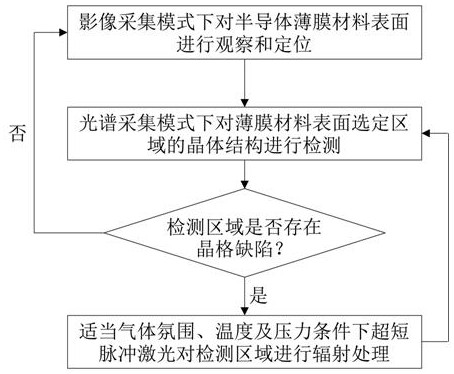
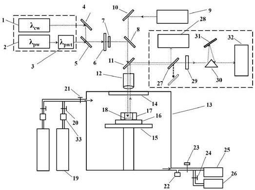
[0030] An embodiment of the present invention provides a device with the functions of crystal structure detection and in-situ repair. The device includes a laser source, a laser optical path system, an illumination light source, an illumination optical path system, an image and spectrum acquisition system, a vacuum system, an air path system, XYZ three-axis translation stage, hot and cold stage, diamond pressure chamber. Such as figure 2 , during the working process of the device, firstly, the image acquisition mode is used to observe and l...


PUM

PropertyMeasurementUnit
sizeaaaaaaaaaa
thicknessaaaaaaaaaa

Abstract

The invention discloses a device with the functions of crystal structure detection and in-situ repair, which uses a continuous laser to excite and collect the scattering spectrum of a semiconductor thin film material, and can quickly and non-destructively judge the crystal quality of the whole and local areas of the semi-thin film material , and then use ultrashort pulse high-energy laser beams such as picoseconds and femtoseconds to irradiate the areas with poor crystal quality in the semiconductor thin film material, thereby stimulating the atoms in the corresponding area of ​​the thin film material to undergo reconstruction, and finally realize the detection of the semiconductor thin film material. In situ repair of crystal structures. Based on the characteristics of short action time of ultrashort pulse laser, small heat-affected range, and high energy density, combined with the control of atmosphere and temperature and pressure conditions, this device can quickly and targetedly repair the surface lattice damage of large-scale semiconductor thin film materials. , to improve its crystal quality, especially suitable for doping semiconductor thin film materials, can effectively improve its uniformity and crystal quality, and optimize the process performance of thin films.

Description

technical field [0001] The invention relates to the field of semiconductor thin film materials, in particular to a device with the functions of crystal structure detection and in-situ repair. Background technique [0002] Chip manufacturing is the driving force for the development of high-tech industries, while semiconductor thin film materials lay the foundation for its development, and have important application prospects in the fields of integrated circuits, high-density storage, display lighting, power electronics, sensors and detectors. With the further development of wide-bandgap semiconductor materials such as diamond, gallium nitride, silicon carbide, and aluminum nitride, modern semiconductor devices are expected to be able to work in harsh environments such as higher frequencies, higher power, and higher temperatures. Higher requirements are also placed on the quality and uniformity of semiconductor thin film materials. In the epitaxial growth and doping process o...

Claims


Application Information

Patent Timeline
Patent Type & Authority Patents(China)
IPC IPC(8): H01L21/67H01L21/02H01L21/268
CPCH01L21/02664H01L21/02686H01L21/268H01L21/67288
Inventor 刘胜吴改汪启军东芳曹强甘志银
Owner WUHAN UNIV
Why Eureka
Try Eureka