

Fully-controlled semiconductor device packaging structure based on integrated commutation
A technology of device packaging and packaging structure, which is applied in the direction of semiconductor devices, electrical components, pulse technology, etc., can solve the problems of extreme working performance and reliability of devices, cost burden and requirements of overall circuit breaker equipment, and achieve high integration , small size, and small stray parameters
- Summary
- Abstract
- Description
- Claims
- Application Information
AI Technical Summary
Problems solved by technology
Method used
Image

Examples
Embodiment Construction
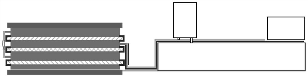
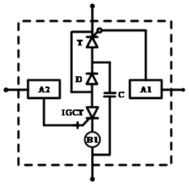
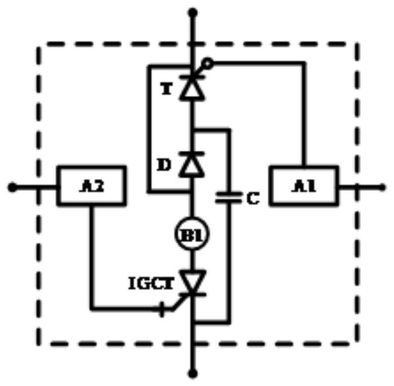
[0032] The following will refer to the attached Figure 1 to Figure 4 Specific embodiments of the present disclosure are described in detail. Although specific embodiments of the present disclosure are shown in the drawings, it should be understood that the present disclosure may be embodied in various forms and should not be limited to the embodiments set forth herein. Rather, these embodiments are provided for more thorough understanding of the present disclosure and to fully convey the scope of the present disclosure to those skilled in the art.
[0033] It should be noted that certain terms are used in the specification and claims to refer to specific components. Those skilled in the art should understand that they may use different terms to refer to the same component. The specification and claims do not use differences in nouns as a way of distinguishing components, but use differences in functions of components as a criterion for distinguishing. "Includes" or "compri...
PUM
 Abstract
Description
Claims
Application Information