Supercharge Your Innovation With Domain-Expert AI Agents!

Optical band frequency-controlled spatio-temporal reconfigurable metamaterial system

A metamaterial and optical band technology, applied in the field of metamaterials, which can solve some problems such as performance impact and complex structure

Pending Publication Date: 2020-12-11
BEIJING INSTITUTE OF TECHNOLOGYGY
View PDF0 Cites 0 Cited by
  • Summary
  • Abstract
  • Description
  • Claims
  • Application Information

AI Technical Summary

Problems solved by technology

[0005] In order to solve the above-mentioned problems in the prior art, that is, in order to solve the problems that the existing active metamaterials based on the combination of metamaterials and semiconductors need to introduce feeder lines, resulting in complex structures and affecting some performances, the present invention provides an optical A time-space reconfigurable metamaterial system with band frequency control, the system includes: a metamaterial structure, which includes no less than two semiconductor material units that respond to light at different frequencies; a light feeding system, which includes no less than two emitting An adjustable light source of light with different frequencies, the light emitting frequency of the adjustable light source corresponds to the type of the semiconductor unit responding to light one by one

Method used


Image

  • Optical band frequency-controlled spatio-temporal reconfigurable metamaterial system
  • Optical band frequency-controlled spatio-temporal reconfigurable metamaterial system
  • Optical band frequency-controlled spatio-temporal reconfigurable metamaterial system

Examples


Embodiment 1

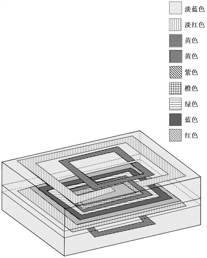
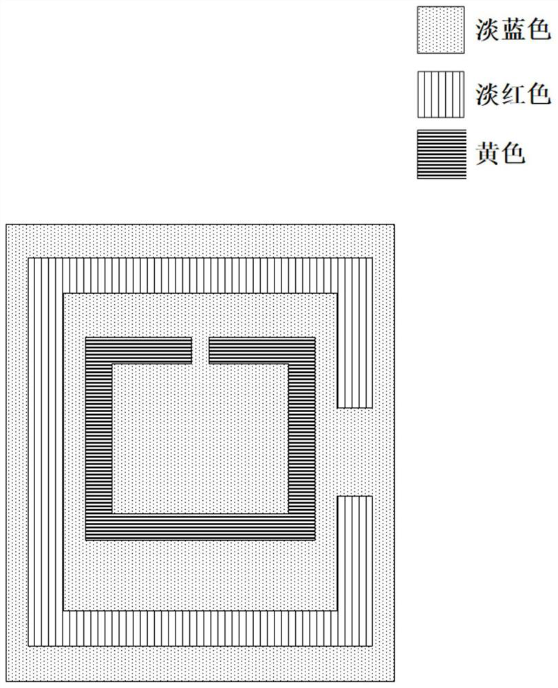
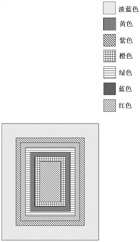
[0053] figure 1 It is a semiconductor material unit composed of three layers of glass vapor-deposited semiconductor, in which light blue represents glass; figure 2 yes figure 1 Schematic diagram of the structure of the upper glass; Figure 3a and Figure 3b yes figure 1 Schematic diagram of the structure of the middle glass; Figure 4a and Figure 4b yes figure 1 Schematic diagram of the structure of the lower glass.

[0054] In the schematic diagram of the upper glass, the material in the light red part is cobalt-doped GaAs, and the material in the yellow part is InAlGaP.

[0055] In the schematic diagram of the middle layer glass, the material of the red part is CH 3 NH 3 Pb(I x Br 1-x ) 3 , the ratio of Br and I is 6:1; the material of the orange part is CH 3 NH 3 Pb(I x Br 1-x ) 3 , the ratio of Br and I is 15:1; the material of the yellow part is CH 3 CH 3 NH 3 PbBr 3 ;The material of the green part is CH 3 NH 3 Pb(Br x Cl 1-x ) 3 , the ratio of...

Embodiment 2

[0061] Figure 7a and Figure 7b The structure shown is a two-dimensional periodic metamaterial structure, which can realize light-controlled frequency-selective absorption of arbitrary polarized waves. Figure 8a and 8b is a structural dimension diagram of the metamaterial structure, and the dimension unit in the diagram is millimeter (mm).

[0062] The material description of each part is as follows:

[0063] The red part represents the light-controlled semiconductor material 1, such as PEDOT:Tos material, which has a conductivity of 1500S / m under red light irradiation, which is hereinafter referred to as "conduction", and has a conductivity of 0.001S / m without red light irradiation. Hereinafter referred to as "non-conductive". The green part represents the light control semiconductor material 2, such as ZnTe:Ga doped Si, the conductivity of this material is 1000S / m under the irradiation of green light, which is hereinafter referred to as "conduction", and the conductivi...

Embodiment 3

[0073] Figure 9a and Figure 9b The structure shown is a two-dimensional periodic metamaterial structure, which can realize light-controlled frequency-selective absorption of arbitrary polarized waves. Figure 10a and 10b is the structural size diagram of the metamaterial structure, the dimensions marked in the diagram are: p=8mm, L=4.53mm, R 1 = 2.1mm, R 2 = 1.7 mm, g 1 =g 2 =0.89mm, W=0.5mm, h 1 = h 2 = 0.035 mm, t = 2 mm.

[0074] The material description of each part is as follows:

[0075] The red part represents the light-controlled semiconductor material 1, such as PEDOT:Tos material, which has a conductivity of 1500S / m under red light irradiation, hereinafter referred to as "conduction", and has a conductivity of 0.001S / m without red light irradiation. Hereinafter referred to as "non-conductive". The green part represents the light-control semiconductor material 3, such as InGaN, which has a conductivity of 300S / m under blue light irradiation and 0.0001S / m und...


PUM

PropertyMeasurementUnit
Conductivityaaaaaaaaaa

Abstract

The invention belongs to the technical field of metamaterials, and aims to solve the problems of complex structure and partial performance influence due to the fact that a feed line needs to be introduced into an existing active metamaterial based on combination of a metamaterial and a semiconductor. To this end, the present invention provides an optical band frequency-controlled spatio-temporal reconfigurable metamaterial system, and the system comprises a metamaterial structure comprising at least two semiconductor material units with different frequency illumination responses; and a light feeding system which comprises at least two adjustable light sources capable of emitting light with different frequencies, wherein the light emitting frequencies of the adjustable light sources correspond to the types of the illumination response semiconductor units one to one. According to the invention, the wireless control of the metamaterial can be realized, the limitation of space wiring of acontrol circuit system needing to be connected due to introduction of a varactor and the like is broken through, and space-time reconstruction control of the metamaterial through illumination of different frequencies is realized; therefore, the metamaterial can be widely applied to electromagnetic shielding, electromagnetic detection, electromagnetic stealth and communication systems.

Description

technical field [0001] The invention belongs to the technical field of metamaterials, and specifically provides a space-time reconfigurable metamaterial system with optical band frequency control. Background technique [0002] Metamaterials refer to composite materials that have artificially designed structures and exhibit extraordinary physical properties that natural materials do not have. Metasurface refers to an artificial layered material whose thickness is smaller than the wavelength. Metasurface can realize the flexible and effective regulation of electromagnetic wave amplitude, phase, polarization (polarization) mode and propagation mode. Metasurface can be regarded as the core of metamaterials. two-dimensional correspondence. [0003] The combination of metasurfaces and semiconductors has brought new opportunities for the development of active metamaterials. How to achieve effective control of semiconductors is the key to the research of this technology. Since cod...

Claims


Application Information

Patent Timeline
IPC IPC(8): H01Q15/00G02B1/00
CPCG02B1/002H01Q15/0086
Inventor 宋巍魏静崔欣葛婷婷井嘉桐盛新庆
Owner BEIJING INSTITUTE OF TECHNOLOGYGY
Features
  • R&D
  • Intellectual Property
  • Life Sciences
  • Materials
  • Tech Scout
  • Unparalleled Data Quality
  • Higher Quality Content
  • 60% Fewer Hallucinations
Learn More