Semiconductor package outer body structure

A semiconductor and outer body technology, applied in the field of semiconductor packaging outer body structure, can solve the problems of difficult alignment of pins, easy shaking, lack of fixed support for installation, etc., to avoid jamming and facilitate welding.

Pending Publication Date: 2020-12-11
容泰半导体(江苏)有限公司
View PDF1 Cites 0 Cited by
  • Summary
  • Abstract
  • Description
  • Claims
  • Application Information

AI Technical Summary

Problems solved by technology

The disadvantage is that when the semiconductor enters the outer body of the package, its pins are difficult to align and enter. At the same time, the installation of the outer body of the package lacks fixed support, and it is easy to shake during use.

Method used


Image

  • Semiconductor package outer body structure
  • Semiconductor package outer body structure
  • Semiconductor package outer body structure

Examples


Embodiment Construction

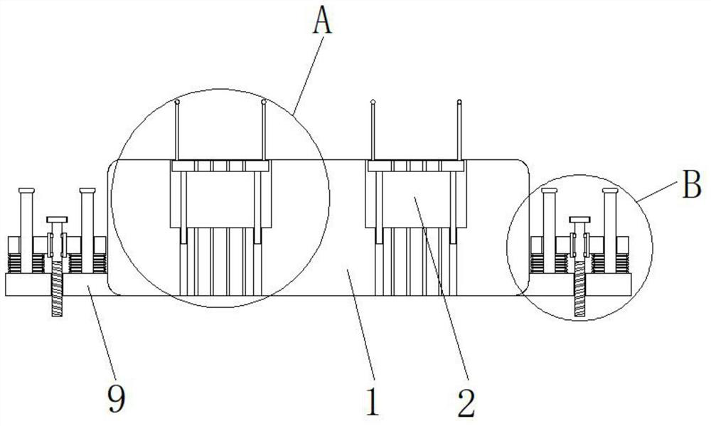
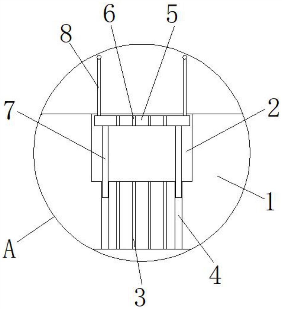
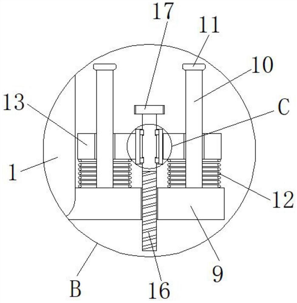
[0023] In order to make the technical means, creative features, goals and effects achieved by the present invention easy to understand, the present invention will be further described below in conjunction with specific embodiments.

[0024] In the description of the present invention, it should be noted that the terms "upper", "lower", "inner", "outer", "front end", "rear end", "both ends", "one end", "another end" The orientation or positional relationship indicated by etc. is based on the orientation or positional relationship shown in the drawings, and is only for the convenience of describing the present invention and simplifying the description, rather than indicating or implying that the referred device or element must have a specific orientation, use a specific Azimuth configuration and operation, therefore, should not be construed as limiting the invention. In addition, the terms "first" and "second" are used for descriptive purposes only, and should not be understood ...


PUM


Abstract

The invention discloses a semiconductor packaging outer body structure, belonging to the field of semiconductor packaging. The semiconductor packaging outer body structure comprises a packaging outerbody, wherein mounting grooves are symmetrically formed in the two sides of the top of the packaging outer body; first pin holes allowing inner cavities of the mounting grooves to communicate with thebottom of the packaging outer body are formed in the wall body of the packaging outer body located at the middle part of the bottoms of the mounting grooves; guiding holes allowing the inner cavitiesof the mounting groove to communicate with the bottom of the packaging outer body are formed in the wall bodies, located at the two sides of the bottoms of the mounting grooves, of the packaging outer body on; bearing plates are arranged at the tops of the inner cavities of the mounting grooves; second pin holes allowing the tops and the bottoms of the bearing plates to be communicated are formedin the middle parts of the bearing plates; and ball head handle rods are symmetrically and fixedly connected to the two sides of the tops of the bearing plates. According to the semiconductor packaging outer body structure, the bearing plates are directionally inserted into the mounting grooves, and the bearing plates drive the pins of a semiconductor to accurately enter the first pin holes and extend to the outer side of the bottom of the packaging outer body, so welding and mounting of the semiconductor are facilitated.

Description

technical field [0001] The invention relates to the field of semiconductor packaging, in particular to a semiconductor packaging outer body structure. Background technique [0002] Taking the motor controller as an example, for the motor controller, the stray inductance of the DC busbar has an important influence on the system efficiency. Especially for the application of wide bandgap semiconductors, low stray inductance can effectively increase the switching speed of semiconductor devices and reduce switching losses. For traditional motor controllers, semiconductor power modules and busbar capacitors are usually designed and manufactured separately, and then connected together by screws or welding during the final assembly process of the motor controller. In this way, although the design of the two is relatively independent, there is no need to over-consider the consistency and versatility of the busbar interface, but such a design method usually makes the stray inductance...

Claims


Application Information

Patent Timeline
Patent Type & Authority Applications(China)
IPC IPC(8): H05K7/12H05K7/10F16F15/067
CPCF16F15/067H05K7/1015H05K7/12
Inventor 马春游
Owner 容泰半导体(江苏)有限公司
Why Eureka
Try Eureka