Multilayer LCP circuit board
A circuit board and copper clad laminate technology, applied in the field of multi-layer LCP circuit boards, can solve the problems of easy occurrence of air bubbles, product deformation, and high fluidity of the substrate, so as to release the pressing stress, reduce the expansion and shrinkage deformation, and improve the good quality. rate effect
- Summary
- Abstract
- Description
- Claims
- Application Information
AI Technical Summary
Problems solved by technology
Method used
Image
Examples
Embodiment Construction
[0018] The present invention will be further described below in conjunction with the accompanying drawings and embodiments.
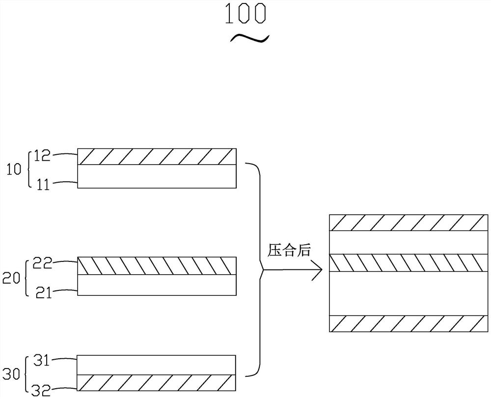
[0019] figure 1 It is a structural schematic diagram of a multi-layer LCP circuit board according to an embodiment of the present invention, please refer to figure 1 The multi-layer LCP circuit board 100 includes a first LCP copper-clad laminate 10 , at least one second LCP copper-clad laminate 20 and a third LCP copper-clad laminate 30 which are stacked in sequence and bonded without glue.
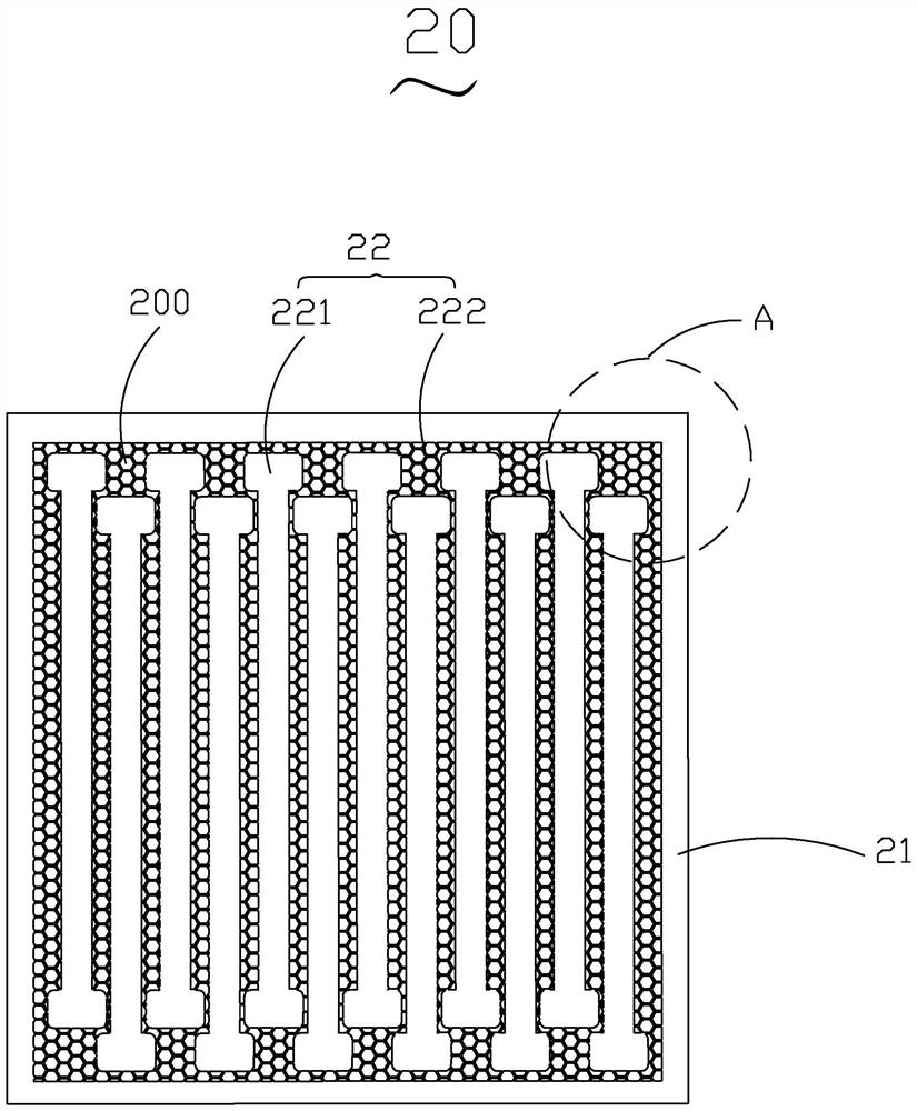
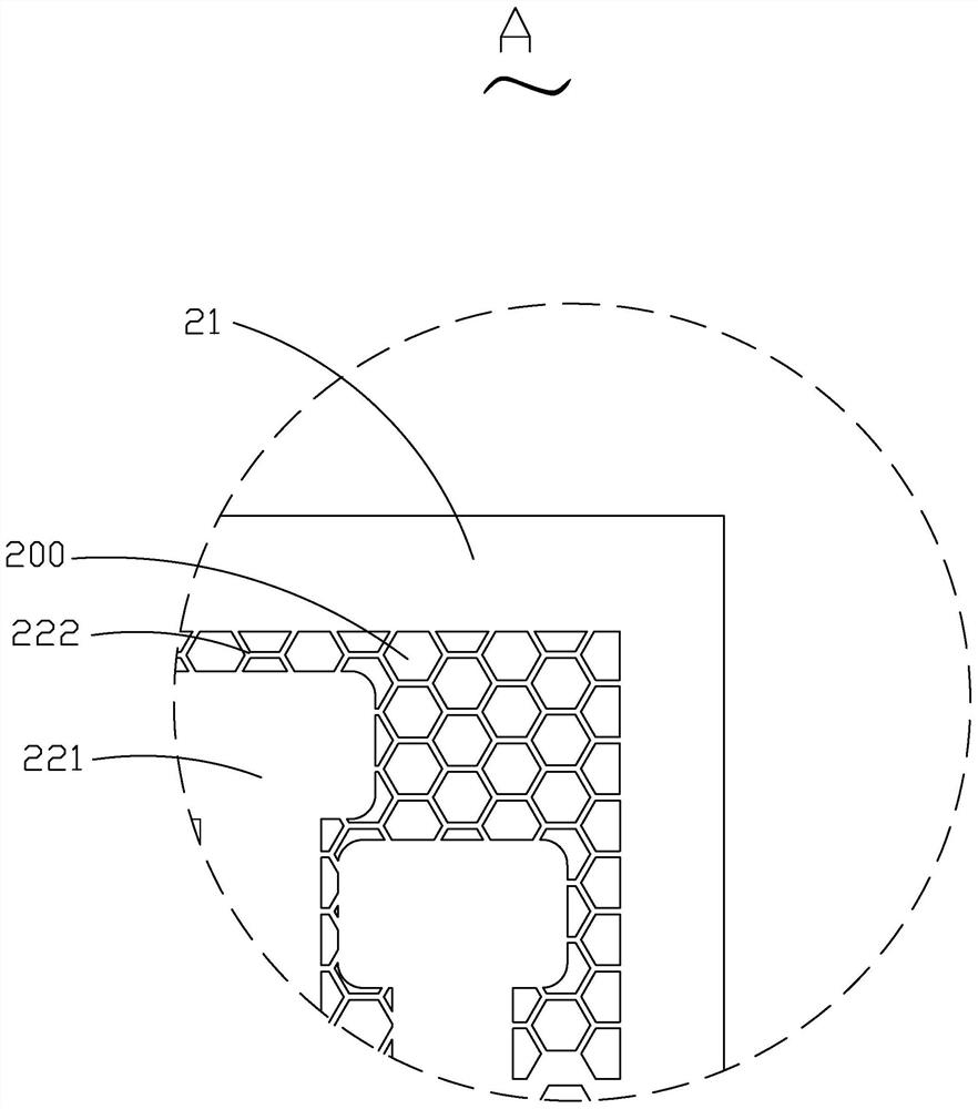
[0020] In this embodiment, when multiple second LCP copper-clad laminates 20 are provided, the multiple second LCP copper-clad laminates 20 have the same structure and are stacked sequentially. In one embodiment, see figure 1 , the second LCP CCL 20 set one, see figure 1 and figure 2 , the second LCP copper clad laminate 20 includes a second LCP layer 21 and a second copper foil layer 22 laminated with the second LCP layer 21 .
[0021] Further, see figure ...
PUM
 Abstract
Description
Claims
Application Information


