Superconducting nanowire structure and preparation method thereof

A technology of superconducting nanowires and substrates, applied in the manufacture/processing of superconductor devices, nanotechnology, nanotechnology, etc., can solve the problems of superconducting nanowire damage, proximity effect of electron beam exposure, etc., to avoid contamination and the effect of etch damage

Pending Publication Date: 2020-12-22
INST OF MICROELECTRONICS CHINESE ACAD OF SCI
View PDF0 Cites 0 Cited by
  • Summary
  • Abstract
  • Description
  • Claims
  • Application Information

AI Technical Summary

Problems solved by technology

[0003] Traditional superconducting nanowire single-photon detectors use a top-down method to realize superconducting nanowires through epitaxial deposition of superconducting materials, electron beam exposure, and etching. Etching will cause damage to superconducting nanowires, and Electron beam exposure also has problems such as proximity effect

Method used


Image

  • Superconducting nanowire structure and preparation method thereof
  • Superconducting nanowire structure and preparation method thereof
  • Superconducting nanowire structure and preparation method thereof

Examples


Embodiment Construction

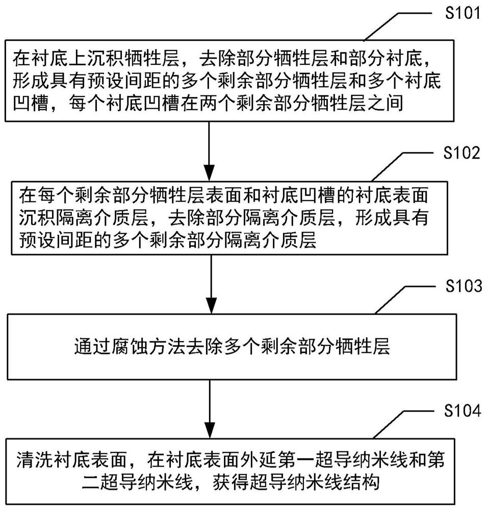
[0026]In order to make the objectives, technical solutions and advantages of the present invention clearer, the present invention will be further described in detail below in conjunction with specific embodiments and with reference to the accompanying drawings. The following embodiments are only used to illustrate the technical solutions of the present invention more clearly, and cannot be used to limit the protection scope of the present invention.

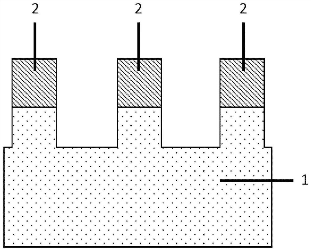
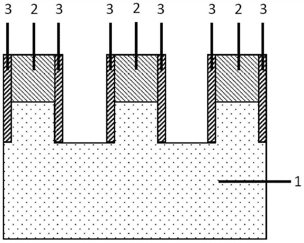
[0027]On the one hand, the purpose of the present invention is to prepare superconducting nanowires in a bottom-up manner, adopting sidewall technology and isolating media for selective epitaxy and isolation of superconducting nanowires, and to provide a superconducting nanowire structure and its Preparation.

[0028]figure 1 A schematic flow chart of a method for preparing a superconducting nanowire structure according to an embodiment of the present invention is schematically shown.

[0029]Such asfigure 1 As shown, the method includes operat...


PUM

PropertyMeasurementUnit
depthaaaaaaaaaa
thicknessaaaaaaaaaa
widthaaaaaaaaaa

Abstract

The invention discloses a superconducting nanowire structure and a preparation method thereof, and provides the preparation method of the superconducting nanowire structure by using a bottom-to-top mode and adopting a side wall technology. The method which comprises the following steps: depositing a sacrificial layer on a substrate, removing part of the sacrificial layer and part of the substrate,forming a plurality of residual sacrificial layers and a plurality of substrate grooves with preset intervals, wherein each substrate groove is arranged between two residual sacrificial layers; depositing an isolation dielectric layer on the surface of each residual sacrificial layer and the surface of the substrate of the substrate groove, and removing a part of the isolation dielectric layer toform a plurality of residual isolation dielectric layers with preset intervals; removing a plurality of residual sacrificial layers through a corrosion method; cleaning the surface of the substrate,and extending the first superconducting nanowire and the second superconducting nanowire on the surface of the substrate to obtain a superconducting nanowire structure.

Description

Technical field[0001]The present invention relates to the field of semiconductor integration technology, in particular to a superconducting nanowire structure and a preparation method thereof.Background technique[0002]As a kind of single-photon detector, superconducting nanowire single-photon detector has the advantages of fast, accurate, high-efficiency, low dark count and corresponding wide spectrum. It has important application prospects and research value in the field of single-photon detection.[0003]The traditional superconducting nanowire single photon detector adopts a top-down method to realize superconducting nanowires through epitaxial deposition of superconducting materials, electron beam exposure, and etching. The etching will cause damage to the superconducting nanowires, and Electron beam exposure also has problems such as proximity effect. How to achieve a high-quality, high-duty-cycle superconducting nanowire structure is a problem that must be considered.Summary of ...

Claims


Application Information

Patent Timeline
Patent Type & Authority Applications(China)
IPC IPC(8): H01L39/02H01L39/24B82Y30/00B82Y40/00
CPCB82Y30/00B82Y40/00H10N60/80H10N60/0128
Inventor 孙兵刘建华刘洪刚常虎东翟明龙
Owner INST OF MICROELECTRONICS CHINESE ACAD OF SCI
Why Eureka
Try Eureka