Method for preparing double-faced growth efficient wide-spectrum absorption multi-junction solar cell

A multi-junction solar cell, double-sided growth technology, applied in circuits, electrical components, final product manufacturing, etc., can solve the problems of material chip warpage, large series resistance, and reduced chip success rate.

Active Publication Date: 2012-10-10
SUZHOU INST OF NANO TECH & NANO BIONICS CHINESE ACEDEMY OF SCI
View PDF4 Cites 10 Cited by
  • Summary
  • Abstract
  • Description
  • Claims
  • Application Information

AI Technical Summary

Problems solved by technology

However, because the lattice mismatch between GaAs material and InP material reaches 3.8%, it is difficult to epitaxially high-quality InP material on GaAs by traditional methods. method to try to realize the quadruple-junction current-matched broad-spectrum absorption cell, however, on the one hand, wafer bonding involves a variety of processes (including layer transfer and chip lift-off technology), which reduces the success rate of the chip; on the other hand, GaAs materials and InP The direct bonding of materials has very high req

Method used


Image

  • Method for preparing double-faced growth efficient wide-spectrum absorption multi-junction solar cell
  • Method for preparing double-faced growth efficient wide-spectrum absorption multi-junction solar cell
  • Method for preparing double-faced growth efficient wide-spectrum absorption multi-junction solar cell

Examples


Embodiment Construction

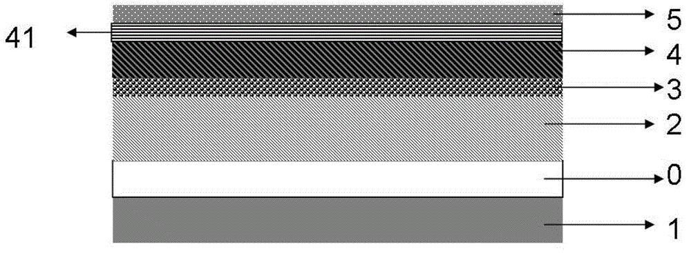
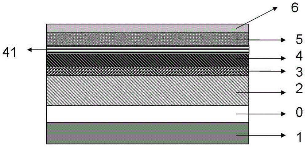
[0028] As mentioned above, the inventor in this case aims to provide a high-efficiency and broad-spectrum absorption multi-junction solar cell manufacturing process to address the shortcomings of the existing multi-junction solar cell manufacturing process. In a nutshell, the present invention applies nanopatterning technology to the epitaxy of GaAs-based InP materials (the lattice mismatch of the two reaches 3.81%, the thermal mismatch is small, and both are zinc blende cubic structures) (GaAs thermal expansion coefficient 5.73 *10 -6 ℃ -1 , InP thermal expansion coefficient 4.6*10 -6 ℃ -1 , the coefficient of thermal expansion of Si is 2.6*10 -6 ℃ -1 , the coefficient of thermal expansion of Ge is 5.9*10 -6 ℃ -1 ), and adopt a double-sided growth method in order not to affect the growth quality of each lattice matching material, so as to obtain GaInP / GaAs / InGaAsP / (InGaAs) wide-spectrum high-efficiency multi-junction cells.

[0029] Further speaking, the process of th...


PUM

PropertyMeasurementUnit
Thicknessaaaaaaaaaa

Abstract

The invention discloses a method for preparing a double-faced growth efficient wide-spectrum absorption multi-junction solar cell. Indium phosphide (InP) extension on a gallium arsenide (GaAs) material and monolithic integration of GaAs and InP cells are realized by using a high depth-to-width ratio dislocation capture technology. The method specifically comprises the following steps of: (1) forming a medium film on a first face of a double-faced polished GaAs substrate, and growing a lattice-matched GaAs/GaInP solar cell structure on a second face of the GaAs substrate; (2) protecting the second face of the substrate, and processing nanoscale medium mask patterns on the first face of the substrate; (3) growing an InP thin film on the first face of the substrate, and polishing the InP thin film until the flatness reaches an extension level; (4) sequentially growing an InGaAsP or InGaAsP/InGaAs solar cell structure and an electrode contact layer on the first face of the substrate; and (5) unprotecting the second face of the substrate, and thus obtaining a target product. The method is simple in process, easy to operate and high in yield, and the influence of lattice mismatch and thermal mismatch in a heterogeneous multi-junction solar cell on the quality and performance of a cell material is effectively eliminated.

Description

technical field [0001] The invention relates to a preparation method of a photovoltaic device, in particular to a preparation method of a double-sided growth high-efficiency broad-spectrum absorption solar cell. Background technique [0002] As a typical way of utilizing solar energy, solar cells have become an important development direction of renewable energy. Improving the efficiency of solar cells is one of the goals pursued by solar cells. III-V group compound semiconductors are ideal for solar cell materials due to their broad energy band structure. GaAs-based III-V group multi-junction cells have been the efficiency record holders and creators in the field of solar cells since their inception. According to the solar spectrum and the band relationship of III-V materials, GaAs-based lattice-matched GaInP / GaAs double-junction cells and InP-based lattice-matched InGaAsP / InGaAs double-junction cells can be reasonably designed to cover most of the sun with current matching...

Claims


Application Information

Patent Timeline
IPC IPC(8): H01L31/18
CPCY02P70/521Y02P70/50
Inventor 张瑞英董建荣杨辉
Owner SUZHOU INST OF NANO TECH & NANO BIONICS CHINESE ACEDEMY OF SCI
Why Eureka
Try Eureka