Method for forming copper layer on circuit board and circuit board with sputtered copper layer

A technology for electroplating copper layers and circuit boards, which is used in printed circuits, printed circuit manufacturing, electrical components, etc., and can solve the problems of high cost of electroless copper plating, complex composition of plating solution, and high process difficulty.

Inactive Publication Date: 2020-12-22
PEI YING SEMICON CO LTD
View PDF5 Cites 2 Cited by
  • Summary
  • Abstract
  • Description
  • Claims
  • Application Information

AI Technical Summary

Problems solved by technology

[0003] However, electroless copper plating also has its disadvantages in that the composition of the plating solution is relatively complex, the process is difficult, and the cost of electroless copper plating is also high.

Method used


Image

  • Method for forming copper layer on circuit board and circuit board with sputtered copper layer
  • Method for forming copper layer on circuit board and circuit board with sputtered copper layer
  • Method for forming copper layer on circuit board and circuit board with sputtered copper layer

Examples


Embodiment Construction

[0018] The invention discloses a method for forming a copper layer on a circuit board and a circuit board with a sputtered copper layer. The method is widely compatible with the copper layer setting process in the existing circuit board manufacturing process, and in particular can replace electroless plating copper process.

[0019] The following pass Figure 1 to Figure 7 The manufacturing process of one embodiment of the present invention is described.

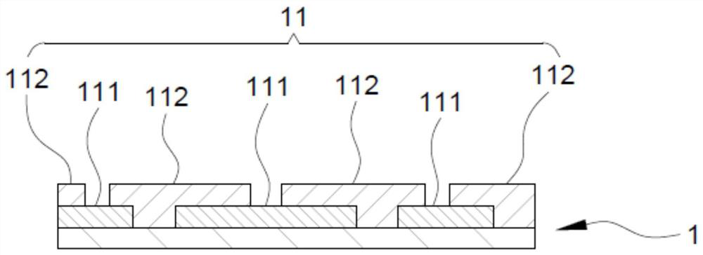
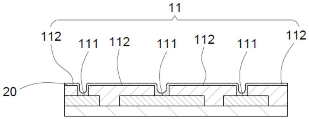
[0020] Please refer to figure 1 , at first, provide a circuit board structure 1, this circuit board structure 1 has a surface 11 to be plated, the surface 11 to be plated has a conductive area 111 and a non-conductive area 112, and the quantity of the conductive area and the non-conductive area 112 depends on the circuit design , in a circuit board structure with high circuit design complexity, the surface 11 to be plated may have a large number of conductive regions 111 and non-conductive regions 112 . It can be understo...


PUM


Abstract

The invention provides a method for forming a copper layer on a circuit board, and the method comprises the steps: providing a circuit board structure which is provided with a to-be-plated surface, wherein the to-be-plated surface is provided with a conductive region and a non-conductive region; and carrying out sputtering treatment on the to-be-plated surface, and forming a sputtering copper layer in the conductive region and the non-conductive region of the to-be-plated surface. According to the invention, a chemical plating process in a circuit board process in the prior art can be replaced.

Description

technical field [0001] The invention relates to a circuit board technology, in particular to a manufacturing process and structure of a copper layer of a circuit board. Background technique [0002] In the current manufacturing process of circuit boards, it is generally necessary to form a copper layer on the substrate by means of electroless plating or electroplating, and the formed copper layer can be further made into a patterned circuit later. Compared with electroplating, electroless plating has the advantage that after proper surface treatment, a thin layer of copper can be plated on the non-conductor surface. This feature greatly improves the freedom of circuit settings, and is widely used in During the circuit board process. [0003] However, electroless copper plating also has its disadvantages in that the composition of the plating solution is relatively complex and the process is difficult, which leads to high cost of electroless copper plating. Contents of the...

Claims


Application Information

Patent Timeline
Patent Type & Authority Applications(China)
IPC IPC(8): H05K3/16
CPCH05K3/16
Inventor 李蕙如
Owner PEI YING SEMICON CO LTD
Why Eureka
Try Eureka