Gate-controlled gallium oxide field effect transistor based on p-i-n structure and its preparation method

A field effect transistor, p-i-n technology, applied in semiconductor/solid-state device manufacturing, semiconductor devices, electrical components, etc., can solve problems such as increasing device static power consumption, low device breakdown voltage, and reducing device reliability. Effects of static loss, improved breakdown voltage, and improved reliability

Active Publication Date: 2022-03-04
XIDIAN UNIV
View PDF8 Cites 0 Cited by
  • Summary
  • Abstract
  • Description
  • Claims
  • Application Information

AI Technical Summary

Problems solved by technology

figure 1 Although the ideal breakdown voltage of the gallium oxide field effect transistor with the horizontal structure shown is very high, the breakdown voltage of the actually prepared device is much lower than the ideal value, and the leakage current is relatively large; in addition, a certain negative gate must be applied. Only when the gate voltage is zero-biased can the device be turned off, that is, the device is not turned off, which reduces the reliability of the device, increases the static power consumption of the device, and limits its application range.

Method used


Image

  • Gate-controlled gallium oxide field effect transistor based on p-i-n structure and its preparation method
  • Gate-controlled gallium oxide field effect transistor based on p-i-n structure and its preparation method
  • Gate-controlled gallium oxide field effect transistor based on p-i-n structure and its preparation method

Examples


Embodiment 1

[0030] Embodiment 1, on the gallium oxide substrate of thickness 300nm, the thickness of making p-type NiO film on the n-type gallium oxide homoepitaxial wafer of thickness 200nm is 200nm, i-Ga 2 o 3 Gallium oxide transistors with a film thickness of 100nm.

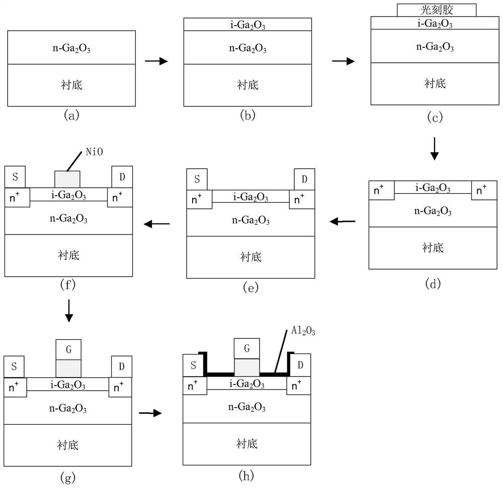
[0031] Step 1, cleaning the epitaxial wafer, such as image 3 (a).

[0032] Select the homoepitaxial gallium oxide epitaxial wafer and clean it, that is, place the homoepitaxial gallium oxide epitaxial wafer in acetone solution and absolute ethanol solution for 5 minutes, then rinse with a large amount of deionized water, and then blow it with nitrogen. Dry.

[0033] Step 2, Deposit i-Ga 2 o 3 film, such as image 3 (b).

[0034] Deposit i-Ga with a thickness of 100nm on the cleaned epitaxial wafer 2 o 3 The thin film layer is then annealed in an oxygen environment, the annealing temperature is 900°C, and the annealing time is 1h, so as to improve the interface contact performance.

[0035] Step 3, photolithogra...

Embodiment 2

[0047] Example 2, SiO with a thickness of 300nm 2 Insulating substrate, n-Ga with a thickness of 200nm 2 o 3 The thickness of the p-type NiO film made on the film is 300nm, i-Ga 2 o 3 Gallium oxide transistors with a film thickness of 120nm.

[0048] Step 1, cleaning the samples, such as image 3 (a).

[0049] 2.1) n-Ga with a thickness of 200nm 2 o 3 Thin films transferred to SiO with a thickness of 300 nm 2 on an insulating substrate;

[0050] 2.2) Put the transferred samples into acetone solution and anhydrous ethanol solution for 8 minutes for ultrasonic cleaning respectively, then rinse with a large amount of deionized water, and then blow dry with nitrogen.

[0051] Step 2, depositing i-Ga 2 o 3 film, such as image 3 (b).

[0052] n-Ga after cleaning 2 o 3 Deposit i-Ga with a thickness of 120nm on the film 2 o 3 The thin film layer is then annealed in an oxygen environment, the annealing temperature is 900°C, and the annealing time is 1h, so as to impro...

Embodiment 3

[0070] Embodiment 3, in the sapphire insulating substrate that thickness is 300nm, the n-Ga that thickness is 200nm 2 o 3 The thickness of the p-type NiO film made on the film is 200nm, i-Ga 2 o 3 Gallium oxide transistors with a film thickness of 80nm.

[0071] Step A, cleaning the sample, such as image 3 (a).

[0072] First, n-Ga with a thickness of 200nm 2 o 3 The thin film layer is transferred to a sapphire insulating substrate with a thickness of 300nm;

[0073] Then, the transferred samples were placed in acetone solution and absolute ethanol solution for 6 min, respectively, for ultrasonic cleaning, rinsed with a large amount of deionized water, and then dried with nitrogen.

[0074] Step B, Deposit i-Ga 2 o 3 film, such as image 3 (b).

[0075] n-Ga after cleaning 2 o 3 Deposit i-Ga with a thickness of 80nm on the film 2 o 3 The thin film layer is then annealed in an oxygen environment, the annealing temperature is 900°C, and the annealing time is 1h, ...


PUM

PropertyMeasurementUnit
thicknessaaaaaaaaaa
thicknessaaaaaaaaaa
thicknessaaaaaaaaaa

Abstract

The invention discloses a gate-controlled gallium oxide field effect transistor based on a p-i-n structure and a preparation method thereof, which mainly solves the problem that the current n-type gallium oxide field effect transistor has a low breakdown voltage and is difficult to turn off. Its bottom-up includes: Ga 2 o 3 Substrate, n‑Ga 2 o 3 An epitaxial layer, the two ends of the upper part of the epitaxial layer are provided with an ion implantation area, and the middle area is provided with a gate electrode; the upper part of the ion implantation area is respectively provided with a source electrode and a drain electrode; the inner surface and the gate electrode are respectively connected to the source electrode and the drain electrode n‑Ga between 2 o 3 Al on top of the epitaxial layer 2 o 3 protective layer; i-Ga between the epitaxial layer and the gate electrode 2 o 3 thin film layer and p-type NiO thin film layer, the p-type NiO thin film layer, i-Ga 2 o 3 thin film layers and n‑Ga 2 o 3 The epitaxial layers form a p‑i‑n structure. The invention improves the performance and reliability of the device and can be used to prepare enhanced gallium oxide devices with high breakdown voltage.

Description

technical field [0001] The invention belongs to the technical field of semiconductor devices, and in particular relates to a gate-controlled gallium oxide field effect transistor, which can be used to prepare high withstand voltage enhanced gallium oxide devices. [0002] technical background [0003] Gallium oxide has five crystal forms of α, β, γ, δ and ε, among which the monoclinic β-Ga 2 O 3 With the best thermal stability, other metastable phases can easily transform into β-Ga at high temperature 2 O 3 , so most of the current research is around β-Ga 2 O 3 Expanded. β-Ga 2 O 3 It has a large forbidden band width (4.4-4.9eV), which makes its ionization rate low and the breakdown field strength is high, about 8MV / cm, which is more than 20 times that of Si and twice that of SiC and GaN many. In addition, β-Ga 2 O 3 The quality factor of Baliga is more than 8 times that of 4H-SiC and more than 4 times that of GaN; the high-frequency Baliga figure of merit is about...

Claims


Application Information

Patent Timeline
Patent Type & Authority Patents(China)
IPC IPC(8): H01L29/78H01L21/336H01L29/06H01L29/24H01L29/423
CPCH01L29/78H01L29/66477H01L29/0611H01L29/24H01L29/4232
Inventor 周弘雷维娜周敏张进成郝跃
Owner XIDIAN UNIV
Why Eureka
Try Eureka