Organic electroluminescent device including hole blocking layer and electron transport layer

An electroluminescent device and device technology, which is applied in the fields of electric solid devices, electrical components, semiconductor devices, etc., can solve the problems of unresearched coordination, unresearched coordination of carbazole compounds, and unconcerned about the coordination of electron transport layer materials, etc. The effect of improving overall performance

Active Publication Date: 2020-12-29
夏禾科技(江苏)有限公司
View PDF22 Cites 0 Cited by
  • Summary
  • Abstract
  • Description
  • Claims
  • Application Information

AI Technical Summary

Problems solved by technology

[0006] U.S. patent application US20190067591A1 discloses a series of compounds with a nitrogen heterocyclic structure such as triazine as the basic skeleton that can be used as hole blocking materials. The matching of electron transport materials with the ring as the basic skeleton, but the coordination of this type of compound as a hole blocking material with other specific structure types, especially electron transport materials containing silicon heterocycles, has not been studied
[0007] Chinese patent application CN 109671851 A discloses a series of carbazole compounds that can be used as hole blocking materials, but this application only studies the combined use of such compounds and three common electron transport materials, and does not study the carbazole compounds Coordination of Compounds as Hole-blocking Materials and Electron-Transporting Materials with Specific Structures
Although the application discloses a series of organic compounds that can be used as hole-blocking layer materials, the application does not pay attention to the coordination of organic compounds as hole-blocking layer materials and electron-transporting layer materials of specific structures.

Method used


Image

  • Organic electroluminescent device including hole blocking layer and electron transport layer
  • Organic electroluminescent device including hole blocking layer and electron transport layer
  • Organic electroluminescent device including hole blocking layer and electron transport layer

Examples


Embodiment 1-1

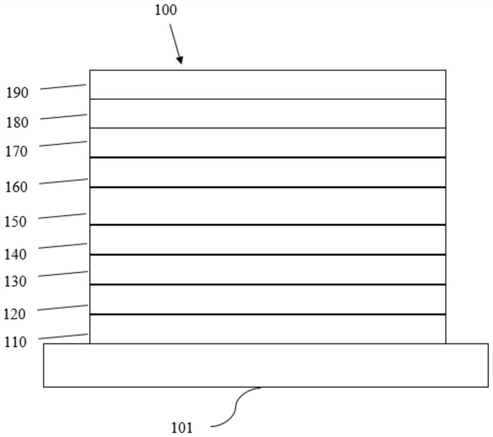
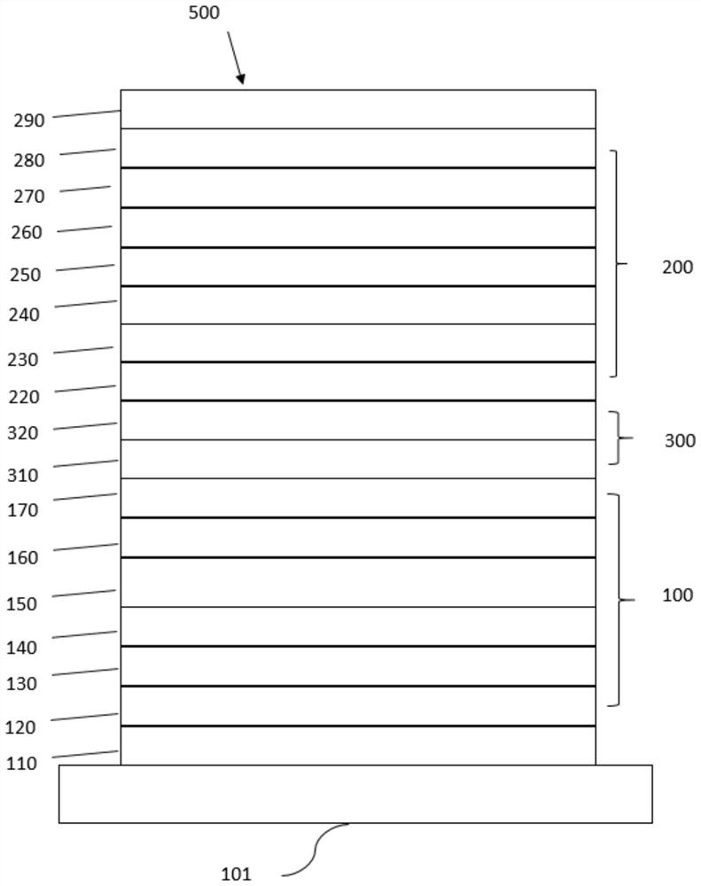
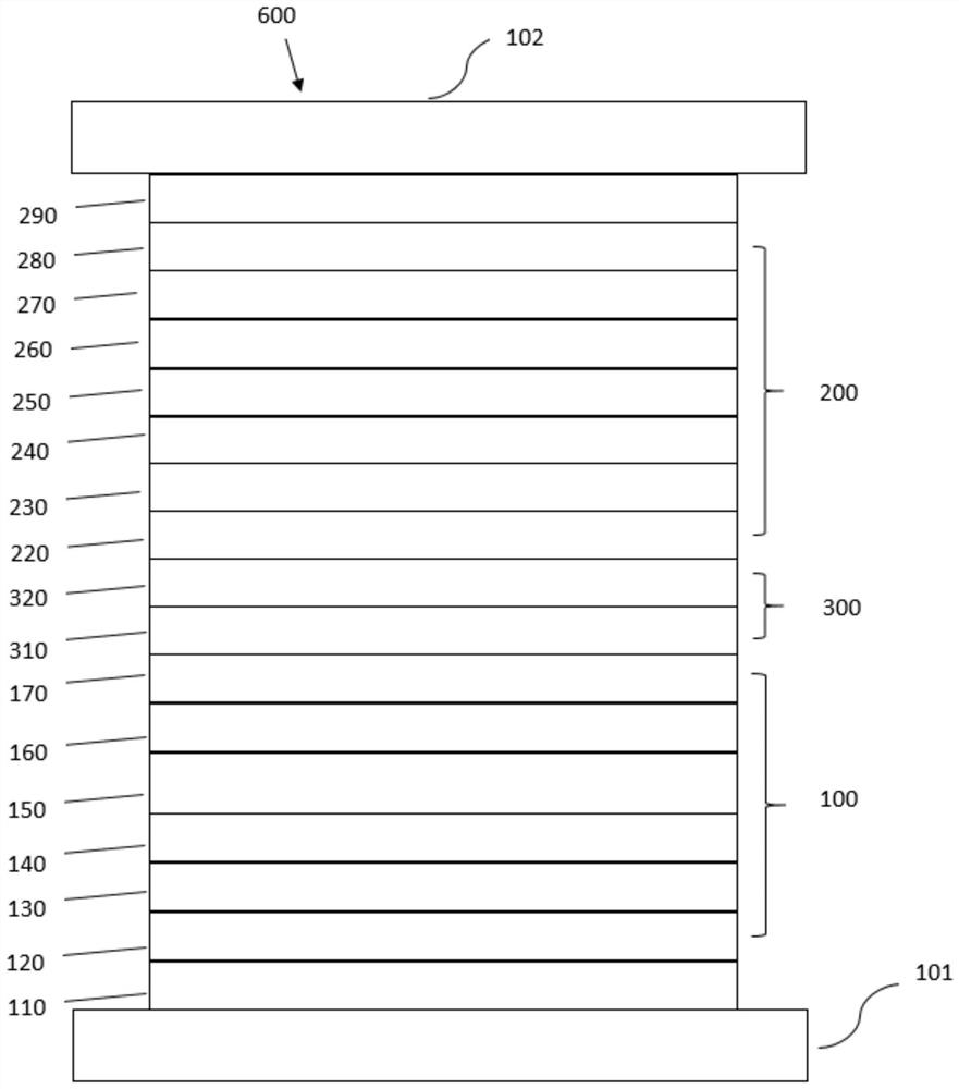
[0188] Example 1-1: Preparation of an organic electroluminescent device comprising the material combination of the present invention.

[0189] First, a glass substrate with an 80 nm thick indium tin oxide (ITO) anode was cleaned and then treated with UV ozone and oxygen plasma. After processing, the substrate was dried in a nitrogen-filled glove box to remove moisture, and then mounted on a substrate holder and loaded into a vacuum chamber. The organic layer specified below, at a vacuum of about 10 -8 Torr's case ends with The rate is sequentially evaporated on the ITO anode by thermal vacuum. Compound HI was used as a hole injection layer (HIL) with a thickness of Compound HT was used as a hole transport layer (HTL) with a thickness of Compound EB was used as an electron blocking layer (EBL) with a thickness of The compound Host1 is used as the host material, the compound D1 is used as the dopant, and the two are co-deposited as the light-emitting layer (EML). The ...


PUM

PropertyMeasurementUnit
emission peakaaaaaaaaaa
thicknessaaaaaaaaaa
thicknessaaaaaaaaaa

Abstract

The invention discloses an organic electroluminescent device including a hole blocking layer and an electron transport layer. The device comprises an anode, a cathode and an organic layer arranged between the anode and the cathode, wherein the organic layer at least comprises a first organic layer and a second organic layer, and both the first organic layer and the second organic layer comprise compounds of specific structures. By selecting a special combination of the hole blocking layer and the electron transport layer containing a specific structural material, the concentration of carriersin the light-emitting layer is effectively regulated and controlled to reach expected balance, and compared with the prior art, the comprehensive performance of the organic light-emitting device is obviously improved. A display assembly is also disclosed.

Description

technical field [0001] The present invention relates to an organic electronic device. More particularly, it relates to organic electroluminescent devices comprising a hole-blocking layer and an electron-transporting layer. Background technique [0002] Organic electronic devices include but are not limited to the following categories: organic light-emitting devices (OLEDs), organic field-effect transistors (O-FETs), organic light-emitting transistors (OLETs), organic photovoltaic devices (OPVs), dye-sensitized solar cells (DSSCs) , organic optical detectors, organic photoreceptors, organic field-effect devices (OFQDs), light-emitting electrochemical cells (LECs), organic laser diodes, and organic plasmonic light-emitting devices. [0003] Organic light-emitting devices have advantages such as wide angle, high contrast ratio and faster response time. Tang and Van Slyke of Eastman Kodak Company reported an organic light-emitting device in 1987, arylamine hole transport layer...

Claims


Application Information

Patent Timeline
Patent Type & Authority Applications(China)
IPC IPC(8): H01L51/50H01L51/54
CPCH10K85/622H10K85/624H10K85/623H10K85/30H10K85/654H10K50/11Y02E10/549
Inventor 王静夏传军邝志远庞惠卿
Owner 夏禾科技(江苏)有限公司
Why Eureka
Try Eureka