Wafer bonding device

A wafer bonding and wafer technology, which is applied in the manufacture of electrical components, electrical solid devices, semiconductor/solid devices, etc., can solve the problems of poor vacuuming effect, low bonding yield, and poor sealing of vacuum chambers, etc., to achieve The effect of fast transmission response, good sealing, and simple connection structure

Pending Publication Date: 2021-01-05
苏州遂芯半导体科技有限公司
View PDF0 Cites 0 Cited by
  • Summary
  • Abstract
  • Description
  • Claims
  • Application Information

AI Technical Summary

Problems solved by technology

Therefore, the sealing of the vacuum chamber is poor, and the vacuuming effect is poor, resulting in a low yield rate of bonding

Method used


Image

  • Wafer bonding device
  • Wafer bonding device
  • Wafer bonding device

Examples


Embodiment Construction

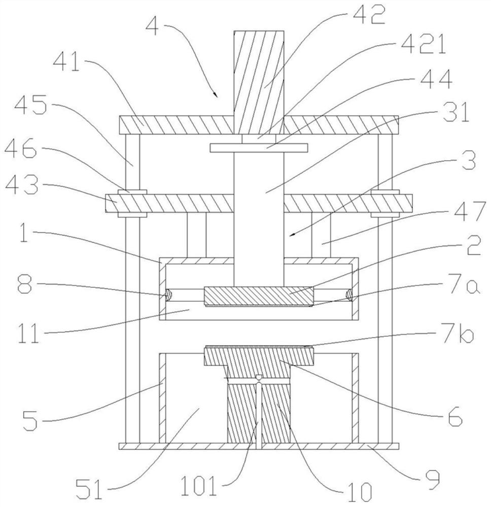
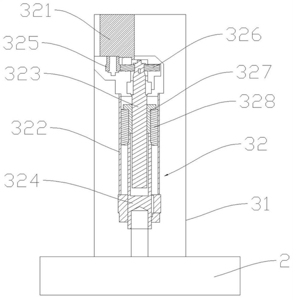
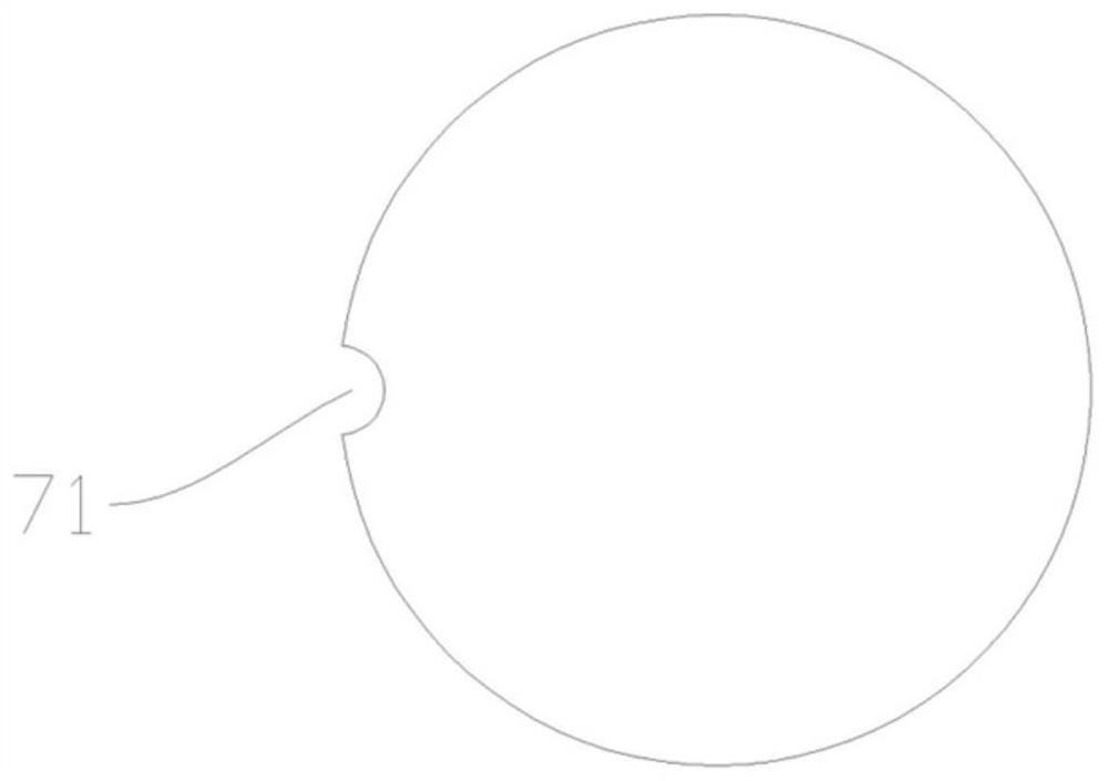
[0020] In order to make the above purpose, features and advantages of the present application more obvious and understandable, the specific implementation manners of the present application will be described in detail below in conjunction with the accompanying drawings. It should be understood that the specific embodiments described here are only used to explain the present application, but not to limit the present application. In addition, it should be noted that, for the convenience of description, only some structures related to the present application are shown in the drawings but not all structures. Based on the embodiments in this application, all other embodiments obtained by persons of ordinary skill in the art without making creative efforts belong to the scope of protection of this application.

[0021] The terms "comprising" and "having" and any variations thereof in this application are intended to cover a non-exclusive inclusion. For example, a process, method, s...


PUM


Abstract

The invention discloses a wafer bonding device. The wafer bonding device comprises: an upper cover body; an upper chuck which is accommodated in the upper cover body and is used for adsorbing the first wafer; a first lifting mechanism which comprises a connecting cylinder tightly arranged in the upper cover body in a penetrating mode, wherein a first driving piece connected with the upper chuck isarranged in the connecting cylinder; a second lifting mechanism which is connected with the connecting cylinder; a lower cover body; and a lower chuck which is accommodated in the lower cover body and is used for adsorbing the second wafer, wherein the lower cover body and the upper cover body are correspondingly arranged, the second lifting mechanism can push the connecting cylinder and can cover the upper cover body on the lower cover body, and the first driving piece can drive the upper chuck to ascend and descend so as to achieve bonding of wafers. The connecting cylinder is tightly arranged in the upper cover body in a penetrating mode, the driving piece for driving the upper chuck to ascend and descend is arranged in the connecting cylinder, and after the upper cover body covers thelower cover body, the sealing performance of a vacuum cavity formed by the upper cover body and the lower cover body is good; the connecting cylinder is connected with the second lifting mechanism, the second lifting mechanism can drive the connecting cylinder to ascend and descend, the connecting structure is simple, and transmission response is fast.

Description

technical field [0001] The invention relates to the technical field of semiconductor manufacturing, in particular to a wafer bonding device. Background technique [0002] Temporary wafer bonding technology refers to the close combination of the front side of the device wafer and the polished carrier wafer through the interposer adhesive through chemical and physical actions. After the wafers are bonded, the bonding interface reaches a specific bonding strength, which plays a good role in mechanical support and protection for the device wafer, so that it can maintain a stable yield rate in subsequent processing and handling. After the process, the device wafer and the carrier wafer are separated from the bonding material (adhesive) interface, and the residual bonding material is removed. [0003] During the bonding process, processes such as vacuuming, heating, applying pressure, cooling and breaking the vacuum are required. The existing wafer bonding device usually has a th...

Claims


Application Information

Patent Timeline
Patent Type & Authority Applications(China)
IPC IPC(8): H01L21/67H01L21/683
CPCH01L21/67121H01L21/6835H01L2221/68304H01L2221/6834
Inventor 邓人仁
Owner 苏州遂芯半导体科技有限公司
Why Eureka
Try Eureka