Multi-cutter wafer splitting device and splitting processing method

A wafer and split technology, applied in the manufacture of electrical components, electrical solid devices, semiconductor/solid devices, etc., can solve the problems of uneven wafer thickness, enlarged stretch film frame, edge chipping, etc., to meet special processing requirements , improve processing efficiency, and ensure the effect of yield

Active Publication Date: 2021-01-08
北京中科镭特电子有限公司
View PDF8 Cites 1 Cited by
  • Summary
  • Abstract
  • Description
  • Claims
  • Application Information

AI Technical Summary

Problems solved by technology

The length of the riving knife needs to be slightly larger than the diameter of the wafer to be produced, which will cause the riving knife to collide with the stretch film frame and cannot contact the wafer for splitting when the dicing line is far away from the center of the circle.
In order to avoid this problem, the inner diameter of the stretch film frame must be increased. For example, a 12-inch stretch film frame is generally used in the industry to carry a 6-inch wafer. Before splitting, the 6-inch wafer needs to be transferred to a 12-inch stretch film frame. , the process is cumbersome, and it is also a great waste of the film used to adhere the wafer
[0006] To sum up, the existing wafer splitting process control is not perfect enough, such as uneven wafer thickness leads to chipping, twins and other defective products. Therefore, a new processing technology is urgently needed

Method used


Image

  • Multi-cutter wafer splitting device and splitting processing method
  • Multi-cutter wafer splitting device and splitting processing method
  • Multi-cutter wafer splitting device and splitting processing method

Examples


Embodiment Construction

[0042] In order to make the purpose, technical solutions and advantages of the embodiments of the present invention clearer, the technical solutions in the embodiments of the present invention will be clearly and completely described below in conjunction with the drawings in the embodiments of the present invention. Obviously, the described embodiments It is a part of embodiments of the present invention, but not all embodiments. Based on the embodiments of the present invention, all other embodiments obtained by persons of ordinary skill in the art without making creative efforts belong to the protection scope of the present invention.

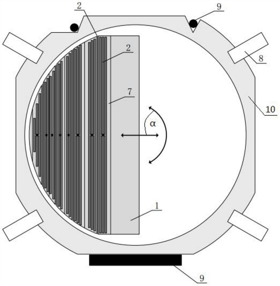
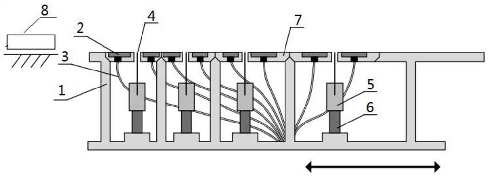
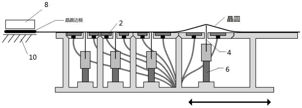
[0043] A wafer splitting device, see his 1- Figure 5 , the device includes a supporting processing table, a processing unit, an adsorption mechanism, a visual detection unit and a control unit (not shown).

[0044] Support the processing table, the support processing table includes a support base (not shown in the figure), a rotation mechan...


PUM


Abstract

The invention discloses a multi-cutter wafer splitting device and a splitting processing method. The device comprises a supporting processing table, an adsorption mechanism, a processing unit, a visual detection unit and a control unit; the processing unit comprises a splitting head support, a plurality of splitting cutter heads, a cutter head fastening device and a lifting valve; the control unitjudges and controls the rotating angle of the rotating mechanism, the clamping force of the wafer clamping mechanism, selection of the splitting cutter heads and the height of the lifting valve according to the information detected by the visual detection unit, and judges and controls the splitting processing state. The method comprises the steps of preprocessing a primarily processed wafer, clamping and positioning the wafer, selecting a tool bit, cracking the wafer, reversing and cracking the wafer and the like until the whole wafer is cracked. According to the wafer splitting device, the multiple splitting cutter heads are adopted, the splitting cutter heads cannot make contact with the front face of the wafer in the pressure applying process, the whole cutting channel is stressed evenly, edge breakage and other defects are not likely to happen, the rate of finished products is guaranteed, in addition, the splitting tool bits are automatically selected through software, and the machining efficiency is improved.

Description

technical field [0001] The invention relates to wafer splitting technology, in particular to a multi-knife wafer splitting device and a splitting processing method. Background technique [0002] In the existing wafer processing technology, the wafer splitting process is to place the pre-cut film-coated wafer in the processing position, and the pre-cutting can be done by laser cutting or knife cutting. The wafer itself is placed on a dedicated film, which is achieved by a wafer laminating machine. The film-coated wafer is placed on the chopping board, and the platform is lifted to apply an external force to the diced wafer through the tension of the film, so that the wafer is split along the dicing road, and then the expanded wafer is fixed. The steps are complete. [0003] Due to the inconsistency of the laser cutting process, the original expansion process can only be applied to wafers with a very good cutting effect, otherwise the expansion machine can only apply transve...

Claims


Application Information

Patent Timeline
Patent Type & Authority Applications(China)
IPC IPC(8): H01L21/67H01L21/683H01L21/687
CPCH01L21/67092H01L21/6838H01L21/68742H01L21/6836H01L2221/68354
Inventor 李纪东易飞跃侯煜李曼张喆王然张紫辰张昆鹏杨顺凯
Owner 北京中科镭特电子有限公司
Why Eureka
Try Eureka