Jig temporary storing mechanism and method for light attenuation resistance treatment of solar silicon wafer

A caching mechanism and silicon wafer technology, applied in photovoltaic power generation, conveyor objects, electrical components, etc., can solve the problems of increasing equipment complexity, positioning fixture caching steps, reducing the quality of solar silicon wafers, and cracking of solar silicon wafers

Inactive Publication Date: 2021-01-19
宁波初创产品设计有限公司
View PDF1 Cites 0 Cited by
  • Summary
  • Abstract
  • Description
  • Claims
  • Application Information

AI Technical Summary

Problems solved by technology

[0004] The prior art has the following deficiencies: when caching redundant positioning fixtures, the redundant positioning fixtures are first moved to the buffering station with a moving device, and then the positioning fixtures on the buffering station are moved with the moving device when needed To the jig output station; and this kind of buffering method requires a moving device to carry when positioning the jig input and output, and the moving device needs to complete the three steps of moving down, grabbing, translational transportation, and j...

Method used


Image

  • Jig temporary storing mechanism and method for light attenuation resistance treatment of solar silicon wafer
  • Jig temporary storing mechanism and method for light attenuation resistance treatment of solar silicon wafer
  • Jig temporary storing mechanism and method for light attenuation resistance treatment of solar silicon wafer

Examples


Embodiment 1

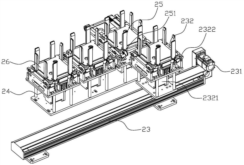
[0026] Such as figure 1 A jig cache mechanism 22 for solar silicon wafer anti-light attenuation treatment shown, the mechanism includes a jig moving assembly 23, a jig storing assembly 24 and a jig output assembly 25; the jig moving assembly 23 input end and the jig The output end of the feeding mechanism 21 is connected, the output end of the jig moving assembly 23 is connected with the input end of the jig output assembly 25; the jig storage assembly 24 is connected with the silicon wafer positioning jig 212, and the output end of the jig storage assembly 24 It is connected with the jig moving assembly 23; the output end of the jig output assembly 25 is connected with the feed port of the light attenuation furnace; the jig moving assembly 23 is used to receive and move solar silicon wafers; the jig storage assembly 24 is used to store excess solar energy Silicon wafer; the jig output assembly 25 is used to output the solar silicon wafer to the light attenuation furnace.

[...


PUM


Abstract

The invention relates to the technical field of solar silicon wafer production, and particularly relates to a jig temporary storing mechanism and method for light attenuation resistance treatment of asolar silicon wafer. The mechanism comprises a jig moving assembly, a jig storage assembly and a jig output assembly, wherein the output end of the jig output assembly is connected with a feeding port of a light attenuation furnace; the jig moving assembly is used for receiving and moving the solar silicon wafer; the jig storage assembly is used for storing redundant solar silicon wafers; and thejig output assembly is used for outputting the solar silicon wafer to the light attenuation furnace. According to the mechanism and method, the jig storage assembly is arranged, so that the temporarystoring step of positioning a jig is reduced, and the quality of the solar silicon wafer in the temporary storing process is improved.

Description

technical field [0001] The invention relates to the technical field of solar silicon wafer production, in particular to a jig buffer mechanism and method for anti-light decay treatment of solar silicon wafers. Background technique [0002] At present, boron-doped P-type crystalline silicon solar cells occupy more than 70% of the photovoltaic market. However, the efficiency of this type of solar cell will decrease when it is used. This phenomenon is called light-induced attenuation. Light attenuation research is to place the silicon wafer under the light source for irradiation, test its electrical properties before and after irradiation and obtain the corresponding light attenuation range. To study the light attenuation of silicon wafers, it is generally to place the silicon wafers in a light attenuation chamber that simulates a solar generator for illumination, and then test the electrical properties of the silicon wafers. When studying the light attenuation of silicon wafe...

Claims


Application Information

Patent Timeline
IPC IPC(8): B65G47/22B65G47/88B65G47/74B65G47/90H01L31/18
CPCB65G47/22B65G47/74B65G47/8815B65G47/901H01L31/1868Y02E10/50Y02P70/50
Inventor 徐建方王凤连王莉霞
Owner 宁波初创产品设计有限公司
Why Eureka
Try Eureka