Solar silicon wafer light attenuation resisting device and anti-light-decay processing method

A technology of silicon wafers and solar energy, applied in photovoltaic power generation, electrical components, climate sustainability, etc., can solve problems such as extrusion collision, misalignment, and low position accuracy of the limit head, so as to improve applicability and limit position Accuracy, avoiding the effect of large offset

Inactive Publication Date: 2021-03-12
宁波初创产品设计有限公司
View PDF1 Cites 2 Cited by
  • Summary
  • Abstract
  • Description
  • Claims
  • Application Information

AI Technical Summary

Problems solved by technology

[0004] The existing technology of silicon wafers silicon wafers silicon wafers silicon wafers has the following deficiencies: 1. When performing light attenuation treatment on solar silicon wafers, each process is manually completed on a single workbench, and then the product flow is sent to the next step through the conveyor line. The workbench carries out the next process processing, and finally completes the entire solar silicon wafer light attenuation treatment process; and each process requires manual participation and auxiliary feeding and transfer, which affects the processing efficiency of the entire device and causes the automation of the entire equipment to a lesser extent
2. When loading solar silicon wafers, two cylinders are used to drive the limit head to move to the position in contact with the two sides of the solar silicon wafer to limit the solar silicon wafers on the conveyor belt; The stroke and the length of the limit head connected to the cylinder are fixed, that is, a group of cylinders and limit heads correspond to a solar silicon wafer of a size; when loading and limiting solar silicon wafers of different specifications, it is necessary to Replacing the length of the limit cylinder or the limit head reduces the applicability of the entire equipment; at the same time, because the manufacturing accuracy of the cylinder is generally low, the position accuracy of the limit head when the cylinder drives the limit head is low; it is easy to cause the limit head to deviate Excessive contact between the limiting position and the solar silicon wafer damages the solar silicon wafer or insufficient contact with the solar silicon wafer cannot limit the position, which is not conducive to the precise positioning of the solar silicon wafer
3. When transporting solar silicon wafers, first move multiple solar silicon wafers to the positioning fixture, and then directly transport the positioning fixtures to the next station through the conveyor belt to complete the solar silicon wafer transportation process; and the silicon wafer positioning fixture In order to ensure that the solar silicon wafer can be placed smoothly, the tool is generally fitted with a gap between the solar silicon wafer, that is, there is a gap between the edge of the solar silicon wafer and the positioning fixture; When in the jig, the upper solar silicon wafer and the lower solar silicon wafer will not be aligned; and because there is no device for sorting the stacked solar silicon wafers, multiple solar silicon wafers are transported and subjected to light attenuation treatment Can not be aligned, resulting in different light attenuation treatment effects of solar silicon wafers in different positions, reducing the quality of light attenuation treatment
4. When buffering redundant positioning fixtures, first use the moving device to move the redundant positioning fixtures to the buffering station, and then use the moving device to move the positioning fixtures on the buffering station to the fixture output station when needed position; and this kind of caching method requires a moving device to carry the input and output of the positioning fixture, and the moving device needs to complete the three steps of moving down and grabbing, translational conveying and fixture falling to complete the buffering of the positioning fixture, thereby increasing the equipment. The complexity and the caching steps of the positioning fixture; at the same time, solar silicon wafers are hard and brittle materials, and the impact force generated during the process of handling, grabbing, moving up and falling may easily cause the stacked solar silicon wafers in the positioning fixture to squeeze and collide with each other ; Thereby causing the solar silicon wafer to crack, reducing the quality of the solar silicon wafer in the caching process

Method used


Image

  • Solar silicon wafer light attenuation resisting device and anti-light-decay processing method
  • Solar silicon wafer light attenuation resisting device and anti-light-decay processing method
  • Solar silicon wafer light attenuation resisting device and anti-light-decay processing method

Examples


Embodiment 1

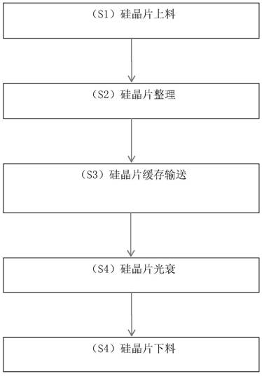
[0039] Such as Figure 1-15 A solar silicon wafer anti-light attenuation equipment shown, the equipment includes a workbench and a silicon wafer feeding device 1 fixed on the workbench, a silicon wafer conveying device 2, a light attenuation furnace 3, a feeding device 4 and fixtures The reflow device 5 is connected to the silicon wafer feeding device 1 and the unloading device 4; the input end and the output end of the silicon wafer feeding device 1 are respectively connected with the silicon wafer feeding port and the silicon wafer conveying device 2 input end; the silicon wafer conveying device 2. The output end is connected to the feed port of the light decay furnace, and the discharge port of the light decay furnace is connected to the feed end of the unloading device; the discharge end of the unloading device is connected to the unloading station; the silicon wafer feeding device 1 is used for The loading of solar silicon wafers; the silicon wafer conveying device 2 is u...


PUM


Abstract

The invention relates to the technical field of solar silicon wafer production. A solar silicon wafer light attenuation resisting device comprises a workbench, a silicon wafer feeding device, a silicon wafer conveying device, a light attenuation furnace and a discharging device. The silicon wafer feeding device, the silicon wafer conveying device, the light attenuation furnace and the dischargingdevice are fixed to the workbench. The input end and the output end of the silicon wafer feeding device are connected with the silicon wafer feeding port and the input end of the silicon wafer conveying device respectively. The output end of the silicon wafer conveying device is connected with a feeding port of the light attenuation furnace, and a discharging port of the light attenuation furnaceis connected with the feeding end of the discharging device. The discharging end of the discharging device is connected with the discharging station. By arranging the silicon wafer feeding device, thesilicon wafer conveying device, the light attenuation furnace and the discharging device, automatic processing and circulation of solar silicon wafers are achieved, and the automation degree of the whole device is improved.

Description

technical field [0001] The invention relates to the field of solar silicon wafers, in particular to a solar silicon wafer anti-light attenuation device and an anti-light attenuation treatment method. Background technique [0002] At present, boron-doped P-type crystalline silicon solar cells occupy more than 70% of the photovoltaic market. However, the efficiency of this type of solar cell will decrease when it is used. This phenomenon is called light-induced attenuation. Light attenuation research is to place the silicon wafer under the light source for irradiation, test its electrical properties before and after irradiation and obtain the corresponding light attenuation range. To study the light attenuation of silicon wafers, it is generally to place the silicon wafers in a light attenuation chamber that simulates a solar generator for illumination, and then test the electrical properties of the silicon wafers. When studying the light attenuation of silicon wafers, it is ...

Claims


Application Information

Patent Timeline
Patent Type & Authority Applications(China)
IPC IPC(8): H01L21/677H01L31/18
CPCH01L21/67742H01L21/6776H01L31/1804H01L31/1868H01L31/1876Y02E10/547Y02P70/50
Inventor 徐建方王凤连王莉霞
Owner 宁波初创产品设计有限公司
Why Eureka
Try Eureka