Solar silicon wafer anti-light-decay processing and conveying device and method

A technology of conveying device and silicon wafer, which is applied to conveyor objects, transportation and packaging, photovoltaic power generation, etc., can solve the problems of different light decay treatment effects of solar silicon wafers, reducing the quality of light decay treatment, and reducing the quality of solar silicon wafers.

Inactive Publication Date: 2021-01-19
宁波初创产品设计有限公司
View PDF1 Cites 0 Cited by
  • Summary
  • Abstract
  • Description
  • Claims
  • Application Information

AI Technical Summary

Problems solved by technology

[0004] The prior art has the following deficiencies: 1. When transporting solar silicon wafers, first move a plurality of solar silicon wafers to the positioning jig, and then directly transport the positioning jigs to the next station through the conveyor belt to complete the solar silicon wafer resistance. Light attenuation processing and conveying process; In order to ensure that the solar silicon wafer can be placed smoothly, the silicon wafer positioning fixture generally cooperates with the solar silicon wafer as a gap, that is, there is a gap between the edge of the solar silicon wafer and the positioning fixture; due to the existence of moving errors, When a plurality of solar silicon wafers are stacked in the silicon wafer positioning fixture, the solar silicon wafers on the top and the solar silicon wafers below will be out of alignment; and because there is no device for organizing the stacked solar silicon wafers, After multiple solar silicon wafers are transported for anti-light attenuation treatment, they cannot be aligned during light attenuation treatment, resulting in different light attenuation treatment effects for solar silicon wafers at different positions, which reduces the quality of light attenuation treatment
2. When buffering redundant positioning fixtures, first use the moving device to move the redundant positioning fixtures to the buffering station, and then use the moving device to move the positioning fixtures on the buffering station to the fixture output station when needed position; and this kind of caching method requires a moving device to carry the input and output of the positioning fixture, and the moving device needs to complete the three steps of moving down and grabbing, translational conveying and fixture falling to complete the buffering of the positioning fixture, thereby increasing the equipment. The complexity and the caching steps of the positioning fixture; at the same time, solar silicon wafers are hard and brittle materials, and the impact force generated during the process of handling, grabbing, moving up and falling may easily cause the stacked solar silicon wafers in the positioning fixture to squeeze and collide with each other ; Thereby causing the solar silicon wafer to crack, reducing the quality of the solar silicon wafer in the caching process

Method used


Image

  • Solar silicon wafer anti-light-decay processing and conveying device and method
  • Solar silicon wafer anti-light-decay processing and conveying device and method
  • Solar silicon wafer anti-light-decay processing and conveying device and method

Examples


Embodiment 1

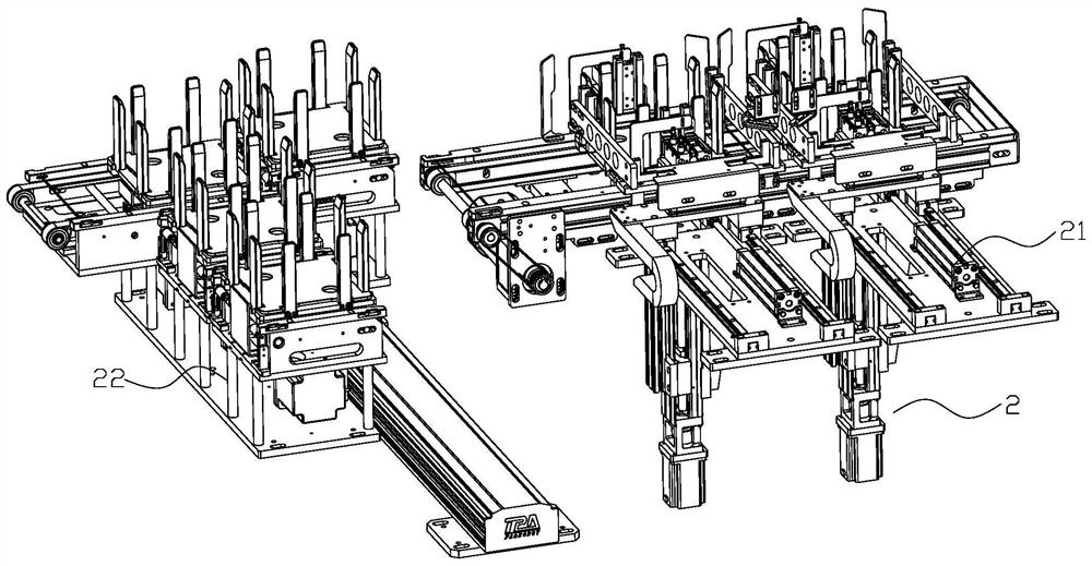
[0031]Such asfigure 1 The silicon wafer conveying device 2 shown includes a fixture feeding mechanism 21 and a fixture buffering mechanism 22; the fixture feeding mechanism 21 and the fixture buffering mechanism 22 are both fixed on the workbench, and the fixture feeding mechanism 21 The input end is connected with the output end of the silicon wafer feeding device 1, and the output end of the jig feeding mechanism 21 is connected with the input end of the jig buffer mechanism 22; the output end of the jig buffer mechanism 22 is connected with the light decay furnace inlet The jig feeding mechanism 21 is used to position and transport the solar silicon wafer; the jig buffer mechanism 22 is used to buffer the transferred surplus jig and output to the next station.

[0032]The product flow direction of solar silicon wafers is from the fixture feeding mechanism 21 to the fixture buffer mechanism 22.

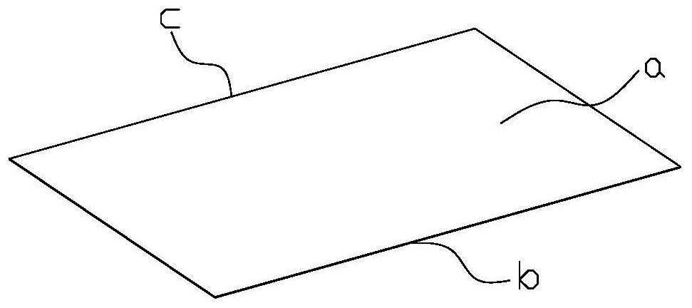
[0033]Such asfigure 2 Shown is a schematic diagram of the product structure of a single sol...


PUM


Abstract

The invention relates to the field of solar silicon wafer production, and discloses a solar silicon wafer anti-light-decay processing and conveying device and method. The solar silicon wafer anti-light-decay processing and conveying device comprises a jig feeding mechanism and a jig caching mechanism. The input end of the jig feeding mechanism is connected with the output end of a silicon wafer feeding device, and the output end of the jig feeding mechanism is connected with the input end of the jig caching mechanism. The output end of the jig caching mechanism is connected with a feed port ofa light decay furnace. The jig feeding mechanism is used for positioning and conveying solar silicon wafers. The jig caching mechanism is used for caching conveyed redundant jigs and then outputtingthe jigs to the next station. According to the solar silicon wafer anti-light-decay processing and conveying device, the stacked solar silicon wafers are sorted by arranging the jig feeding mechanism,and the quality of light decay treatment is improved; and by arranging the jig caching mechanism, the caching step of positioning the jigs is reduced, and the quality of the solar silicon wafers in the caching process is improved.

Description

Technical field[0001]The invention relates to the technical field of solar silicon wafer production, in particular to a solar silicon wafer anti-light decay processing and transportation device and method.Background technique[0002]At present, boron-doped P-type crystalline silicon solar cells account for more than 70% of the photovoltaic market. However, when this type of solar cell is used, the efficiency will decrease, which is called light-induced attenuation. The light attenuation research is to irradiate the silicon wafer under a light source, test its electrical properties before and after irradiation, and obtain the corresponding light attenuation amplitude. Research on the light attenuation of silicon wafers is generally to place the silicon wafers in a light attenuation box that simulates a solar generator for illumination, and then test the electrical properties of the silicon wafers. When studying the light attenuation of silicon wafers, the solar silicon wafers need to b...

Claims


Application Information

Patent Timeline
Patent Type & Authority Applications(China)
IPC IPC(8): B65G47/74B65G47/22B65G47/88B65G47/90H01L31/18
CPCB65G47/22B65G47/74B65G47/8815B65G47/901H01L31/1868Y02E10/50Y02P70/50
Inventor 徐建方王凤连王莉霞
Owner 宁波初创产品设计有限公司
Why Eureka
Try Eureka