Withstand voltage test device for semiconductor production
A withstand voltage test and semiconductor technology, which is applied in the field of withstand voltage test devices for semiconductor production, can solve the problems of easy electric shock, threat to the safety of operators, and the influence of semiconductor withstand voltage test, so as to avoid pressure damage and ensure the accuracy of withstand voltage test Effect
- Summary
- Abstract
- Description
- Claims
- Application Information
AI Technical Summary
Problems solved by technology
Method used
Image
Examples
Embodiment 1
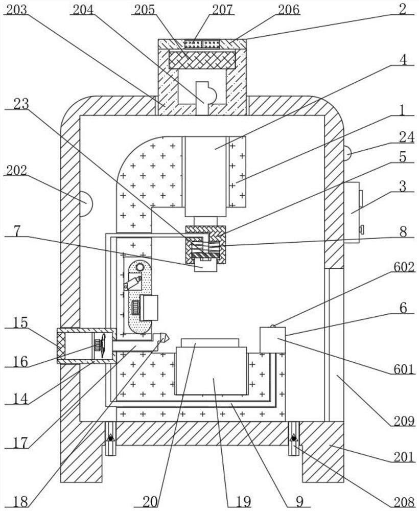
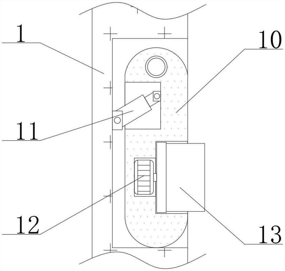
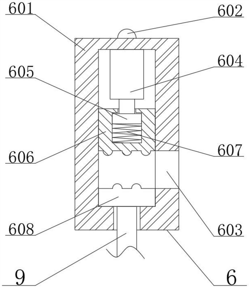
[0025] see figure 1 , figure 2 , image 3 , Figure 4 with Figure 5 , the present invention provides a technical solution:
[0026]A withstand voltage test device for semiconductor production, comprising a fixed frame 1, a protective device 2 and a connecting device 6, the outer side of the fixed frame 1 is provided with a protective device 2, the protective device 2 includes a protective box 201, and the outer side of the fixed frame 1 is fixedly connected with a protective box 201, a humidity sensor 202 is fixedly connected to the upper left inside of the protective box 201, a drying box 203 is fixedly connected to the top of the protective box 201, and the drying box 203 runs through the protective box 201, and an air pump 204 is connected to the inner side of the bottom end of the drying box 203, and the inside of the drying box 203 The top is slidingly connected with a drying filter 205, and the inner side of the box cover 206 is fixedly connected with a rubber bloc...
Embodiment 2
[0029] The same parts as those in Embodiment 1 will not be repeated in Example 2, but the difference is that the left end of the fixed frame 1 is connected with a bellows 14, and the bellows 14 runs through the protective device 2, and the bellows 14 is fixedly connected with the protective device 2, and the inside of the bellows 14 The adsorption filter screen 15 and fan 16 are fixedly connected to the left and right. The right end of the bellows 14 is connected with the air pipe 17, and the other end of the air pipe 17 is connected with the nozzle 18. The inclination angle of the nozzle 18 is 30°. Before the semiconductor is tested, the contact block and the semiconductor can be cleaned, thereby avoiding the phenomenon that a large amount of dirt attached to the outside of the contact block caused by long-term use will affect the test. By cleaning the dust and foreign objects outside the semiconductor, it is also avoided. The phenomenon of crushing ensures the accuracy of the...
PUM
 Abstract
Description
Claims
Application Information


