Electroplating-chemical plating integrated process for ultra-thin wafer

A wafer, ultra-thin technology, applied in the direction of metal material coating process, circuits, electrical components, etc., can solve the problems of very high requirements on metal surface characteristics, unfavorable thick-layer electroplating film production, affecting the effect of chemical plating, etc. Reduce the risk of fragmentation, avoid the effects of natural oxidation or contamination

Pending Publication Date: 2021-01-22
绍兴同芯成集成电路有限公司
View PDF12 Cites 0 Cited by
  • Summary
  • Abstract
  • Description
  • Claims
  • Application Information

AI Technical Summary

Problems solved by technology

[0003] Electroless plating, also known as electroless plating, is characterized by using the potential difference between the metal on the surface of the substrate and the electrolyte to naturally and spontaneously generate electrochemical reactions without external electrodes and current. The advantage is that it can achieve selective growth, only The metal part reacts, only the insulator part does not react at all, so the pattern distribution of the electroplating area can be formed without the yellow light pattern, but because the film thickness reaches a certain level, the ion exchange speed will slow down, which is not conducive to The production of thick electroplating film, in addition, electroless plating has very high requirements on the characteristics of the metal surface, any natural oxide layer and organic matter or other pollution will seriously affect the effect of subsequent electroplating, for this situation, combined with electrode The characteristics of electroplating and electroless electroplating, integrated process and equipment to achieve the most efficient and yield integrated wafer and glass carrier process, now proposes an ultra-thin wafer electroplating, electroless plating integrated process

Method used


Image

  • Electroplating-chemical plating integrated process for ultra-thin wafer

Examples


Embodiment 1

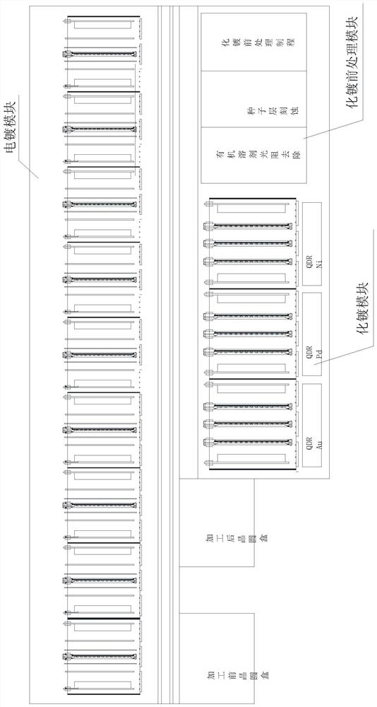
[0032] The ultra-thin wafer bonded to the glass carrier or the ultra-thin wafer with a gentle slope edge, the wafer is horizontally transferred to the ring clamp joint area, and the semi-circular clamp is used to combine the thicker edge of the ultra-thin wafer (gentle slope or The thicker part around the stepped edge wafer) is fixed with a ring-shaped fixture. The fixture is designed with a connection point with the external power supply, which can evenly distribute the current to the wafer surface through the ring-shaped fixture. The fixture fixes the ultra-thin wafer, and the ultra-thin wafer is connected to the power contact point of the electroplating tank, and the electroplating process starts. After the electroplating is completed, the ring-shaped fixture fixes the ultra-thin wafer and enters the rotating spray chamber to complete the photoresist removal. The step is to carry out the pretreatment process of seed layer etching and electroless plating. The pretreatment pro...


PUM


Abstract

The invention discloses an electroplating-chemical plating integrated process for an ultra-thin wafer. The process comprises the following steps: bonding an ultra-thin wafer of a glass carrier plate or an ultra-thin wafer with a gentle slope-shaped edge, jointing the ultra-thin wafer with a power supply contact point of an electroplating bath, starting an electroplating process, fixing the ultra-thin wafer into a rotary spraying cavity by an annular clamp after electroplating is finished, removing a photoresist, conducting a pretreatment process of seed layer etching and chemical plating, allowing the annular clamp to continue to fix the ultrathin wafer, enabling the clamped ultrathin wafer to enter a chemical plating tank, carrying out various metallization plating processes separately, cleaning and drying the annular clamp and the ultrathin wafer, and separating the annular clamp from the ultrathin wafer. According to the electroplating-chemical plating integrated process for the ultrathin wafer, horizontal / vertical matching, rotating and soaking matching of process equipment can be achieved to achieve optimal process efficiency, the ultrathin wafer is continuously conveyed and positioned in different types of reaction tanks to complete each process, and natural oxidation or pollution during intervals is avoided.

Description

technical field [0001] The invention relates to the field of semiconductor technology, in particular to an ultra-thin wafer electroplating and electroless plating integration process. Background technique [0002] Semiconductor 3D components or MEMS (micro-electromechanical systems) or high-end high-power devices, combined with ultra-thin wafers and glass substrates, use TSV and TGV to connect upper and lower components to form fast, low-loss, and good heat dissipation 2.5D, 3D components, It is necessary to combine the advantages and characteristics of electroless plating and electroplating to achieve perfect metal connection and bonding. [0003] Electroless plating, also known as electroless plating, is characterized by using the potential difference between the metal on the surface of the substrate and the electrolyte to naturally and spontaneously generate electrochemical reactions without external electrodes and current. The advantage is that it can achieve selective g...

Claims


Application Information

Patent Timeline
Patent Type & Authority Applications(China)
IPC IPC(8): H01L21/683H01L21/02C23C28/00
CPCH01L21/6835H01L21/02697C23C28/00H01L2221/68372
Inventor 严立巍文锺符德荣
Owner 绍兴同芯成集成电路有限公司
Why Eureka
Try Eureka