Hydrofluoric acid etching solution for etching gallium indium zinc oxide film and application thereof

A technology of gallium indium zinc oxide and hydrofluoric acid, applied in the direction of surface etching compositions, chemical instruments and methods, electrical components, etc., can solve the problem of large loss of the lower tunneling layer, unstable properties of the etching solution, and uncontrollable etching speed etc. to achieve the effect of slow etching speed, stable etching process and controllable etching speed

Inactive Publication Date: 2021-02-02
SHANDONG SINOCHIP SEMICON
View PDF6 Cites 0 Cited by
  • Summary
  • Abstract
  • Description
  • Claims
  • Application Information

AI Technical Summary

Problems solved by technology

[0006] Aiming at the problems in the prior art that the etchant of the IGZO film etchant has a fast etching speed, the etching speed is uncontrollable, the loss of the lower tunneling layer is large, and the properties of the etchant are unstable, the present invention discloses a method for etching gallium indium zinc oxide thin films. Hydrofluoric acid etching solution, the composition of the etching solution is simple, it can be diluted when used, the etching speed is controllable, and the loss of the lower oxide layer is small

Method used


Image

  • Hydrofluoric acid etching solution for etching gallium indium zinc oxide film and application thereof
  • Hydrofluoric acid etching solution for etching gallium indium zinc oxide film and application thereof
  • Hydrofluoric acid etching solution for etching gallium indium zinc oxide film and application thereof

Examples


Embodiment 1

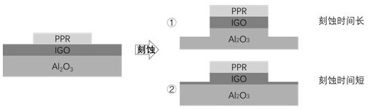
[0023] (1) Select a heavily doped p-type silicon wafer as the substrate, and use magnetron sputtering equipment to deposit 10nm aluminum oxide (Al 2 o 3 ), and then in Ar atmosphere, magnetron sputtering deposited 15nm gallium indium zinc oxide (IGZO) film with a mass ratio of 1:1:1, and the radio frequency power was 70W, which was used as the experimental material;

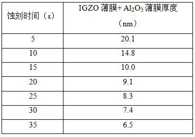
[0024] (2) Dilute the concentrated hydrofluoric acid solution with a concentration of 40% plus deionized water to 100 times, and then immerse the multiple experimental materials prepared in step (1) in the diluted hydrofluoric acid solution at 25°C, respectively Last for 5 seconds, 10 seconds, 15 seconds, 20 seconds, 25 seconds, 30 seconds and 35 seconds, take it out, rinse it with deionized water and dry it, and measure the thickness of alumina with an ellipsometer. The results are shown in Table 1 Show.

[0025] Table 1 shows the residual thickness of the aluminum oxide layer under different etching times. It...

Embodiment 2

[0030] (1) Select a heavily doped p-type silicon wafer as the substrate, and use magnetron sputtering equipment to deposit 10nm aluminum oxide (Al 2 o 3 ), and then in Ar atmosphere, magnetron sputtering deposited 15nm gallium indium zinc oxide (IGZO) film with a mass ratio of 1:1:1, and the radio frequency power was 70W, which was used as the experimental material;

[0031] (2) Dilute the concentrated solution of hydrofluoric acid with a concentration of 20% plus deionized water to 100 times, and then immerse the multiple experimental materials prepared in step (1) in the diluted solution of hydrofluoric acid at 25°C, respectively Last for 8 seconds, 16 seconds, 24 seconds, 32 seconds, 40 seconds, 48 ​​seconds, 56 seconds, take it out, rinse it with deionized water and dry it, then use an ellipsometer to measure the thickness of alumina, the results are shown in Table 2 Show.

[0032] Table 2 shows the residual thickness of the aluminum oxide layer under different etching t...

Embodiment 3

[0037] (1) Select a heavily doped p-type silicon wafer as the substrate, and use magnetron sputtering equipment to deposit 10nm aluminum oxide (Al 2 o 3 ), and then in Ar atmosphere, magnetron sputtering deposited 15nm gallium indium zinc oxide (IGZO) film with a mass ratio of 1:1:1, and the radio frequency power was 70W, which was used as the experimental material;

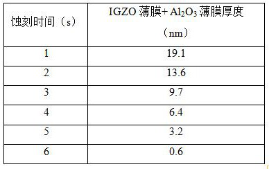
[0038] (2) Dilute the concentrated hydrofluoric acid solution with a concentration of 10% plus deionized water to 10 times, and then immerse the multiple experimental materials prepared in step (1) in the diluted solution of hydrofluoric acid at 25°C, respectively Last for 1 second, 2 seconds, 3 seconds, 4 seconds, 5 seconds, 6 seconds, take it out, rinse it with deionized water and dry it, then use an ellipsometer to measure the thickness of alumina. The results are shown in Table 3.

[0039] Table 3 shows the residual thickness of the aluminum oxide layer under different etching times, and the etching time of ...


PUM

PropertyMeasurementUnit
thicknessaaaaaaaaaa
thicknessaaaaaaaaaa

Abstract

The invention discloses a hydrofluoric acid etching solution for etching a gallium indium zinc oxide film and application thereof, the mass percentage concentration of hydrofluoric acid is 0.2-1%, andthe etching temperature is at room temperature 20-30DEG C. The hydrofluoric acid etching solution is applied to the processing process of a transistor or a flash memory unit taking gallium indium zinc oxide as a communication layer, and particularly, the gallium indium zinc oxide film is deposited on the Al2O3 tunneling layer film as a communication layer. According to the method, the etching process is relatively stable, the formed surface is relatively smooth, the etching speed of the tunneling layer (Al2O3) on the lower layer of gallium indium zinc oxide is low, the caused loss is small, and the stability and high efficiency of the gallium indium zinc oxide device unit are maintained under the condition of low loss. The hydrofluoric acid etching solution can be used immediately after being prepared, so that the problems of unstable properties and short storage time of the mixed acid etching solution are solved.

Description

technical field [0001] The invention belongs to the technical field of semiconductor integrated circuits, and in particular relates to a hydrofluoric acid etchant for etching a gallium indium zinc oxide film and an application thereof. Background technique [0002] Professor Hosono of Tokyo Institute of Technology reported amorphous gallium indium zinc oxide (IGZO) semiconductor transistors in 2004. Due to the carrier mobility 20 to 30 times higher than that of crystalline silicon, and the low preparation temperature and low leakage current, it has attracted much attention. It is often used as a communication layer in transistors or flash memory cells. It is used in the processing of gallium indium zinc oxide devices. Among them, since there are multiple device units on the same substrate, and the channels between them are independent or group independent, the correct etching and separation of the channel parts is the fundamental operation method for forming these independen...

Claims


Application Information

Patent Timeline
Patent Type & Authority Applications(China)
IPC IPC(8): C09K13/08H01L21/465
CPCC09K13/08H01L21/465
Inventor 王萱孙中琳刘尚刘大铕
Owner SHANDONG SINOCHIP SEMICON
Why Eureka
Try Eureka