Design method of thin film transistor

A technology of thin film transistors and design methods, applied in the field of semiconductor transistor devices, to achieve the effect of simple operation and resource saving

Pending Publication Date: 2021-02-02
INST OF MICROELECTRONICS CHINESE ACAD OF SCI
View PDF0 Cites 1 Cited by
  • Summary
  • Abstract
  • Description
  • Claims
  • Application Information

AI Technical Summary

Problems solved by technology

However, although the structure of thin film transistor devices is simple, the factors that affect its characteristics are diverse, and th

Method used


Image

  • Design method of thin film transistor
  • Design method of thin film transistor

Examples


Embodiment Construction

[0018]In order to make the objectives, technical solutions and advantages of the present invention clearer, the present invention will be further described in detail below in conjunction with specific embodiments and with reference to the accompanying drawings.

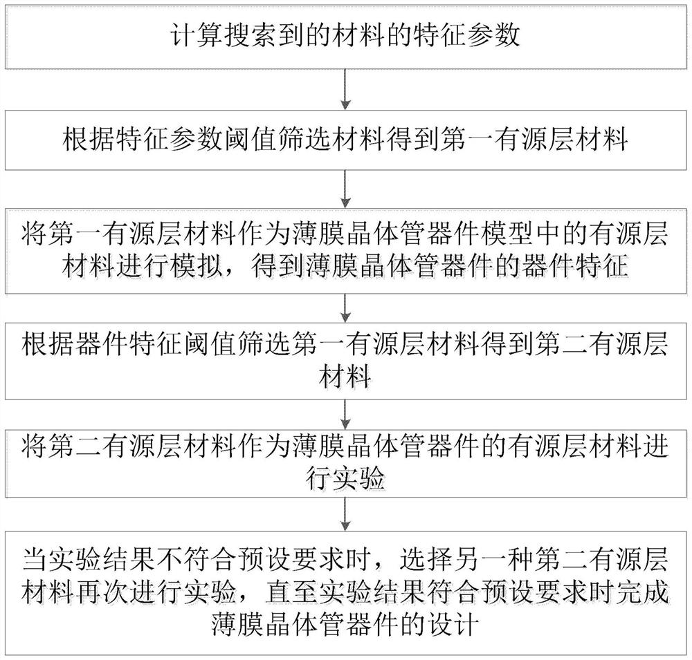
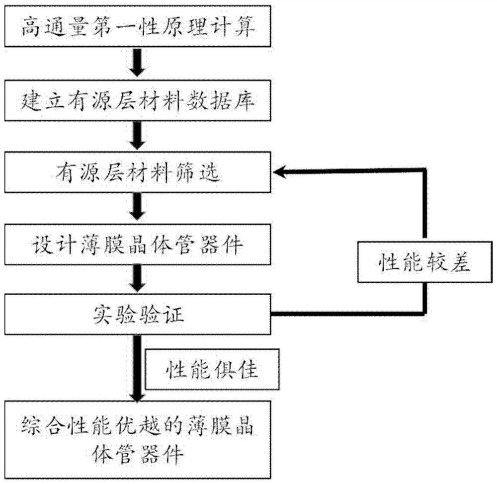
[0019]The present invention proposes a design method for thin film transistor devices based on the analysis of the status quo of related research fields, based on high-throughput integration and first-principles calculation methods. This method is simple to operate and can be widely used in various materials and structures. The design of thin film transistor devices.

[0020]In layman's terms, high-throughput integrated computing is a method of submitting large batches of computing tasks at once, through element substitution, high-throughput screening, structure optimization, and related property calculations to theoretically predict potential new structures and new formulas. The design of high-performance thin-film transistor de...


PUM


Abstract

The invention discloses a design method of a thin film transistor. The method comprises the following steps: calculating characteristic parameters of a searched material; screening materials accordingto the characteristic parameter threshold value to obtain a first active layer material; simulating by taking the first active layer material as an active layer material in the thin film transistor device model to obtain device characteristics of the thin film transistor device; screening the first active layer material according to the device characteristic threshold to obtain a second active layer material; taking the second active layer material as an active layer material of the thin film transistor device for an experiment; and when the experiment result does not meet the preset requirement, selecting another second active layer material to carry out the experiment again, and completing the design of the thin film transistor device until the experiment result meets the preset requirement. According to the method, a large number of physical properties related to the active layer material of the thin film transistor device and a corresponding active layer material database can be obtained through a simple method, and theoretical guidance is provided for researching the characteristics of the thin film transistor device.

Description

Technical field[0001]The invention relates to the field of semiconductor transistor devices, in particular to a method for designing thin film transistors.Background technique[0002]As a useful supplement to field effect transistors, thin film transistors have been widely used in display, sensing and other fields in recent years. Compared with field-effect transistors, thin-film transistors are made of various types of semiconductor materials, and the manufacturing process is relatively simple, and relatively inexpensive large-area spin coating, printing, etc. can be used, so the manufacturing cost is relatively low. In addition, the film material can be made under lower temperature conditions, so materials with poor heat resistance (such as plastic paper and other substrates) can be selected to manufacture electronic devices with light weight, toughness and bendable characteristics. However, due to the wide variety of materials used to make thin film transistor devices, there are st...

Claims


Application Information

Patent Timeline
IPC IPC(8): G06F30/20G16C60/00
CPCG16C60/00G06F30/20
Inventor 卢年端李泠姜文峰耿玓王嘉玮刘明
Owner INST OF MICROELECTRONICS CHINESE ACAD OF SCI
Why Eureka
Try Eureka