Test method of semiconductor memory

A test method and semiconductor technology, applied in static memory, instruments, etc., can solve problems such as hardware detection errors, insufficient coverage, poor control of substandard products, etc., to reduce error rates, enhance promotional value, and coverage wide effect

Pending Publication Date: 2021-02-05
深圳市博业诚电子有限公司
View PDF0 Cites 0 Cited by
  • Summary
  • Abstract
  • Description
  • Claims
  • Application Information

AI Technical Summary

Problems solved by technology

[0004] The purpose of the present invention is to provide a test method for semiconductor memory, which solves the problem that the current test method for semiconductor memory does not have enough scope for hardware detection in the semiconductor processing process, there are errors in hardware detection, and the control degree of unqualified products is not good Waiting question

Method used


Image

  • Test method of semiconductor memory

Examples


Embodiment Construction

[0028] The following will clearly and completely describe the technical solutions in the embodiments of the present invention with reference to the accompanying drawings in the embodiments of the present invention. Obviously, the described embodiments are only some, not all, embodiments of the present invention. Based on the embodiments of the present invention, all other embodiments obtained by persons of ordinary skill in the art without creative efforts fall within the protection scope of the present invention.

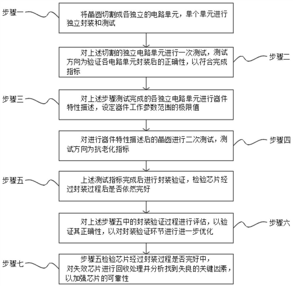
[0029] The invention relates to a test method for a semiconductor memory, including DC test, functional test and AC test. The DC test verifies the voltage and current parameters of the semiconductor, the functional test verifies a series of logical functional operations inside the chip and their correctness, and the AC test verifies the Ensure that the chip can complete logic operations within specific time constraints.

[0030] Depend on figure 1 As shown, the te...


PUM


Abstract

The invention discloses a test method of a semiconductor memory, and relates to the technical field of semiconductor memory test. The invention comprises a DC test, a function test and an AC test, theDC test verifies voltage and current parameters of a semiconductor, the function test verifies a series of logic function operations and correctness thereof in a chip, and the AC test ensures that the chip can complete the logic operations within a specific time constraint. The test method of the semiconductor memory is higher in detection precision of semiconductor hardware, wider in detection link involved range, and capable of effectively reducing the error rate and improving the product yield.

Description

technical field [0001] The invention relates to the technical field of semiconductor memory testing, in particular to a semiconductor memory testing method. Background technique [0002] Semiconductor memory is a solid-state electronic device for storing data information made by semiconductor integrated circuit technology. It is composed of a large number of identical storage units and input and output circuits. Each storage unit has two different representational states "0" and "1". ", used to store different information, semiconductor memory is an important part of the computer, compared with magnetic memory, semiconductor memory has the advantages of fast access speed, large storage capacity, small size, etc., and the memory cell array and the main peripheral logic circuit Compatible and can be made on the same chip, which greatly simplifies the input and output interfaces. Therefore, in terms of high-speed computer storage, semiconductor memory has completely replaced th...

Claims


Application Information

Patent Timeline
Patent Type & Authority Applications(China)
IPC IPC(8): G11C29/00
CPCG11C29/006
Inventor 林汉忠
Owner 深圳市博业诚电子有限公司
Why Eureka
Try Eureka