Flash removal device after integrated circuit packaging
A technology for integrated circuits and packaging devices, which is applied in the field of flash removal devices after integrated circuits are packaged. It can solve problems such as high labor intensity, poor welding of integrated circuits, and impact on product quality, and achieve the effect of saving costs.
- Summary
- Abstract
- Description
- Claims
- Application Information
AI Technical Summary
Problems solved by technology
Method used
Image
Examples
Embodiment Construction
[0028] The following will clearly and completely describe the technical solutions in the embodiments of the present invention with reference to the accompanying drawings in the embodiments of the present invention. Obviously, the described embodiments are only some, not all, embodiments of the present invention. Based on the embodiments of the present invention, all other embodiments obtained by persons of ordinary skill in the art without making creative efforts belong to the protection scope of the present invention.
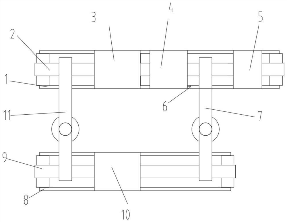
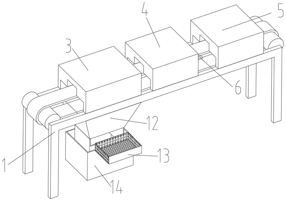
[0029] see Figure 1-2 , the present invention provides a technical solution: after the integrated circuit is packaged, the flash removal device includes a flash removal support 1, which is characterized in that: a flash removal conveyor belt 2 is installed in the middle of the flash removal support 1, and the top left of the flash removal support 1 A high-pressure water flushing box 3 is installed on the side, and a multi-directional high-pressure nozzle is ins...
PUM
 Abstract
Description
Claims
Application Information


