Liquid crystal display panel

A liquid crystal display panel, glass substrate technology, applied in nonlinear optics, instruments, optics, etc., can solve problems such as white point coordinate shift

Inactive Publication Date: 2021-02-19
NANJING CEC PANDA LCD TECH
View PDF6 Cites 0 Cited by
  • Summary
  • Abstract
  • Description
  • Claims
  • Application Information

AI Technical Summary

Problems solved by technology

[0004] image 3 shown respectively for figure 1 and figure 2 The result diagram of the chromaticity simulation, after adding the flat layer 25, the box thickness (optical path difference) at the color layer changes, and the brightness ratio of RY, GY, BY changes, which leads to the offset of the white point coordinates

Method used


Image

  • Liquid crystal display panel
  • Liquid crystal display panel
  • Liquid crystal display panel

Examples


no. 1 example

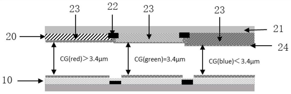
[0024] Such as Figure 4 As shown, the liquid crystal display panel includes an array substrate 10 and a color filter substrate 20 disposed opposite to each other, and a liquid crystal (not shown) located between the array substrate 10 and the color filter substrate 20 .

[0025] The array substrate 10 includes a first glass substrate 11, scan lines 12 and data lines 13 arranged in criss-cross arrangement on the glass substrate 11, a gate insulating layer (not shown) covering the scan lines 12, and a gate insulating layer located on the gate insulating layer. A semiconductor layer (not shown), an organic insulating layer 14 covering the scan lines 12 and data lines 13 , and a pixel electrode 15 on the organic insulating layer 14 .

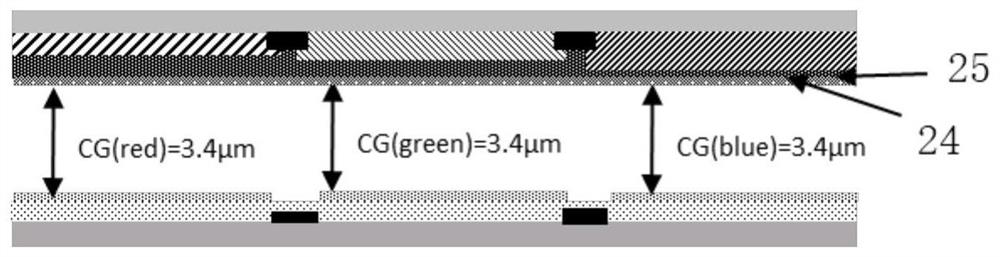
[0026] The color filter substrate 20 includes a second glass substrate 21, a black matrix 22 on the second glass substrate 21, a plurality of colored layers between adjacent black matrices 22, and a flat layer 24 covering the black matrix 22 and th...

no. 2 example

[0032] The difference from the first embodiment above is: H1>H2>H3, H1-H2=0.01 μm˜0.3 μm, H2-H1=0.01 μm˜0.3 μm.

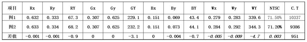
[0033] The cell thickness of the display area of ​​the liquid crystal display panel is: the cell thickness CG(red)3.4μm, to increase the Wx value and Wy value of the panel (WX and WY are the coordinates of the white point).

[0034] The present invention forms organic insulating layers with inconsistent heights by exposing half-tone masks to achieve the purpose of adjusting the thickness of boxes corresponding to areas of different color layers and adjusting the chromaticity of panels.


PUM


Abstract

The invention provides a liquid crystal display panel. The liquid crystal display panel comprises an array substrate and a color film substrate, wherein the array substrate comprises a first glass substrate, a scanning line, a data line, an organic insulating layer and a pixel electrode located on the organic insulating layer, the color film substrate comprises a second glass substrate, black matrixes located on the second glass substrate, a plurality of color layers located between the adjacent black matrixes and flat layers covering the black matrixes and the color layers, the color layers comprise a red color layer, a green color layer and a blue color layer, the organic insulating layer is formed by exposing a halftone photomask, the height of the organic insulating layer in an area corresponding to the red color layer is H1, the height of the organic insulating layer in an area corresponding to the green color layer is H2, the height of the organic insulating layer in an area corresponding to the blue color layer is H3, and H2 is more than H1 and less than H3. According to the invention, the organic insulating layers with inconsistent heights are formed through exposure of thehalftone photomask, so that different box thicknesses of areas corresponding to different color layers are adjusted, and the purpose of adjusting the chromaticity of the panel is achieved.

Description

technical field [0001] The invention relates to the technical field of panel display, in particular to a liquid crystal display panel. Background technique [0002] figure 1 It is a structural schematic diagram of a liquid crystal display panel. The liquid crystal display panel includes an array substrate 10 and a color filter substrate 20 arranged oppositely. The color filter substrate 20 includes a black matrix 22 on a glass substrate 21 and a color layer between adjacent black matrices 22. 23 and the transparent electrode 24 covered on the black matrix 22 and the color layer 23, the color layers 23 are red color layer, green color layer and blue color layer respectively. Both the array substrate 10 and the color filter substrate 20 are provided with red pixel units (red), green pixel units (green) and blue pixel units (blue) that are oppositely arranged. For the film thickness of the color layer of the color filter substrate, the film thickness of the red color layer<...

Claims


Application Information

Patent Timeline
IPC IPC(8): G02F1/1333
CPCG02F1/133345
Inventor 李淑君
Owner NANJING CEC PANDA LCD TECH
Why Eureka
Try Eureka