
Manufacturing method of PMOS

A manufacturing method and wafer technology, which is applied in semiconductor/solid-state device manufacturing, electrical components, circuits, etc., can solve the problems of inability to dynamically adjust different silicon chips, and the inability to improve the performance uniformity of chip and chip devices, so as to improve the on-chip Uniformity, the effect of improving uniformity

Pending Publication Date: 2021-02-19
SHANGHAI HUALI INTEGRATED CIRCUTE MFG CO LTD
View PDF0 Cites 0 Cited by
  • Summary
  • Abstract
  • Description
  • Claims
  • Application Information

AI Technical Summary

Problems solved by technology

The existing SMT RTA adjustment method can only be used for the whole batch (lot) of products, and cannot be dynamically adjusted for different silicon wafers in the same batch, so the uniformity of device performance between wafers cannot be improved.

Method used


Image

  • Manufacturing method of PMOS
  • Manufacturing method of PMOS

Examples


Embodiment Construction

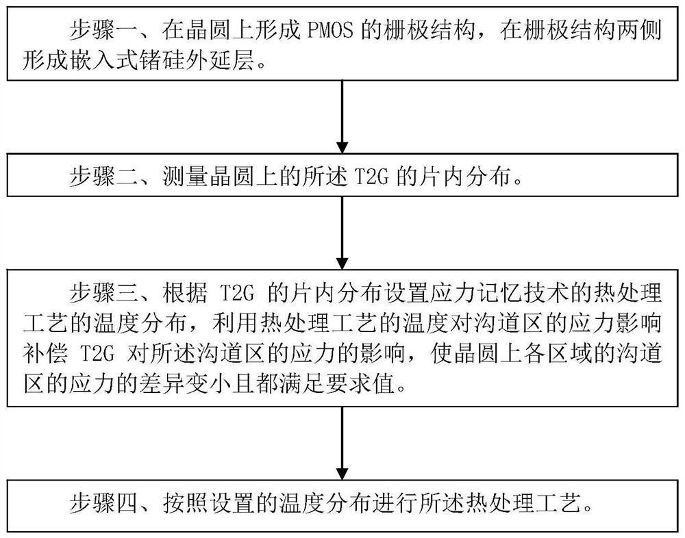
[0045] Such as figure 1 Shown is the flowchart of the manufacturing method of the PMOS embodiment of the present invention; the manufacturing method of the PMOS embodiment of the present invention includes the following steps:

[0046] Step 1. Form a PMOS gate structure on the wafer, and form an embedded silicon-germanium epitaxial layer on both sides of the gate structure. The embedded silicon-germanium epitaxial layer is formed in the groove, and T2G is the embedded silicon-germanium epitaxial layer. The distance between the tip of the silicon germanium epitaxial layer and the gate structure; the wafer is composed of a semiconductor substrate, and a plurality of the PMOSs are integrated on the wafer, and the semiconductor covered by the gate structure A channel region is formed on the surface of the substrate.

[0047] In the embodiment of the present invention, the gate structure is formed by stacking a gate dielectric layer and a polysilicon gate, and the forming steps of t...


PUM


Abstract

The invention discloses a manufacturing method of a PMOS, and the method comprises the following steps of 1, forming a grid structure of the PMOS on a wafer, and forming embedded germanium-silicon epitaxial layers at the two sides of the grid structure; 2, measuring the on-chip distribution of a T2G on the wafer; 3, setting the temperature distribution of a heat treatment process of a stress memory technology according to the on-chip distribution of the T2G, and compensating the influence of the T2G on the stress of a channel region by utilizing the stress influence of the temperature of the heat treatment process on the channel region so as to enable the difference of the stress of the channel region of each region on the wafer to be reduced and meet a required value; and 4, carrying outthe heat treatment process according to the set temperature distribution. The method can achieve the timely dynamic adjustment of the PMOS product of the wafer, and can improve the uniformity of the saturated source and drain currents in the chips, between the chips and between the batches of the product.

Description

technical field [0001] The invention relates to the field of semiconductor integrated circuit manufacturing, in particular to a PMOS manufacturing method. Background technique [0002] In order to improve the performance of PMOS, such as the saturated source-drain current (Idsat), the stress memory technology (SMT), which increases the stress of the channel region, is used in the prior art. The SMT of PMOS is formed by embedded germanium in the source and drain regions. The silicon epitaxial layer is then subjected to the SMT heat treatment process on the silicon germanium epitaxial layer to conduct the stress of the silicon germanium epitaxial layer into the channel region, thereby increasing the mobility of hole carriers in the channel region, and finally making the device Idsat increases, thereby improving device performance. [0003] In the existing PMOS manufacturing method, it is easy to make the Idsat of the PMOS uneven within the same wafer, between different wafers...

Claims


Application Information

Patent Timeline
IPC IPC(8): H01L21/336H01L21/66H01L29/78
CPCH01L29/66492H01L22/12H01L29/7848
Inventor 张庆李中华
Owner SHANGHAI HUALI INTEGRATED CIRCUTE MFG CO LTD
Learn More