Laser-induced printing method of solar cell grid lines based on double groove structure of silicon wafer

A solar cell and laser-induced technology, applied in circuits, electrical components, photovoltaic power generation, etc., can solve problems such as grid line width fluctuations, achieve stable width, reduce production costs, and save silver paste

Active Publication Date: 2022-03-29
SOUTH CHINA UNIV OF TECH
View PDF4 Cites 0 Cited by
  • Summary
  • Abstract
  • Description
  • Claims
  • Application Information

AI Technical Summary

Problems solved by technology

[0004] So far, LIFT technology has proved that it can be applied to the front polarization of solar cells, but due to the limitation of the transfer mechanism, only grid lines with a width of more than 40 μm can be obtained, the aspect ratio of the grid lines is about 0.5, and the obtained grid line width There will be slight fluctuations, fluctuations in ±5μm

Method used


Image

  • Laser-induced printing method of solar cell grid lines based on double groove structure of silicon wafer
  • Laser-induced printing method of solar cell grid lines based on double groove structure of silicon wafer
  • Laser-induced printing method of solar cell grid lines based on double groove structure of silicon wafer

Examples


Embodiment Construction

[0036] The present invention will be further described in detail below in conjunction with specific embodiments.

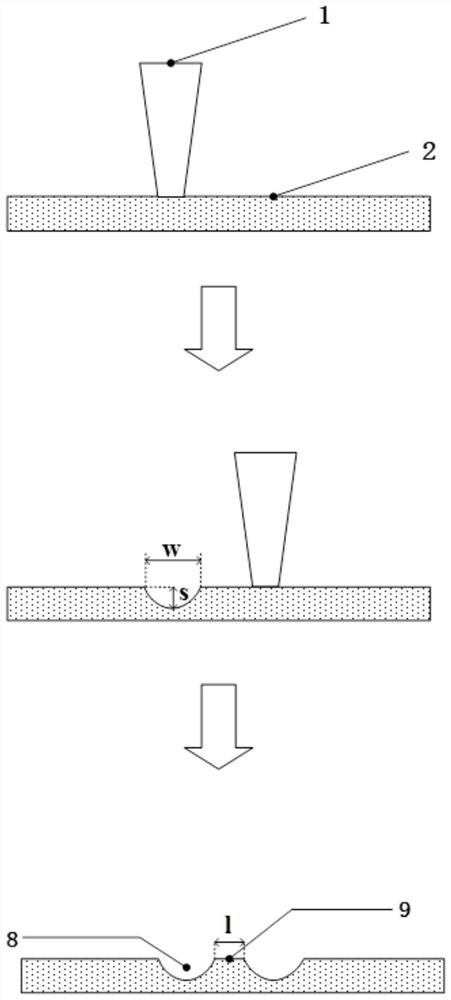
[0037] The specific steps of the laser-induced printing method for solar cell grid lines based on the silicon wafer double groove structure implemented in this embodiment include:

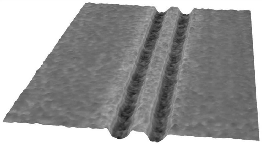
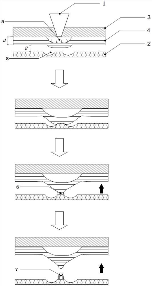
[0038] Step 1: Laser etching the double groove structure to limit the gate line printing area: Before the texturing of the silicon wafer 2, use the laser 1 to etch the left and right two grooves 8 at the predetermined printing position of the gate line on the silicon wafer 2. A certain distance l is maintained between the grooves 8. like Figure 1-2 shown, the groove depth is s and the groove width is w. At this time, the two groove-restricted areas 9 are the predetermined grid line printing areas, and the subsequent printing of the grid lines 7 will be limited in this area.

[0039] Step 2: Preparation of silver paste film: apply the silver paste on the front side of the solar cell...


PUM

PropertyMeasurementUnit
depthaaaaaaaaaa
widthaaaaaaaaaa
thicknessaaaaaaaaaa

Abstract

The invention discloses a laser-induced printing method for grid lines of solar cells based on a double-groove structure on a silicon wafer, which includes: using a laser to etch a double-groove structure on a silicon wafer to limit the grid line printing area, and using a laser to induce a silver paste film A silver paste bridge is generated between the transparent substrate and the double-groove confinement area, and the laser is scanned along the extending direction of the groove interval area, thereby realizing the expansion of the silver paste bridge. The silver paste bridge is stretched by moving the transparent substrate vertically until the silver paste bridge breaks, and finally the gate line with high precision and high aspect ratio is obtained on the silicon wafer. Compared with the traditional screen printing technology, the invention can reduce the cost and reduce the breakage rate. Compared with the original laser-induced transfer method, due to the existence of the grooves, the contact area between the silver paste and the silicon wafer is limited to the interval between the grooves. Therefore, a grid line with a more stable width, higher precision and higher aspect ratio can be obtained.

Description

technical field [0001] The invention relates to a solar cell grid line laser induced printing method based on a silicon wafer double groove structure, in particular to a method for realizing photovoltaic solar cell grid line printing by utilizing a laser induced forward transfer technology (Laser induced forward transfer, LIFT for short). The method belongs to the field of laser application and photovoltaic technology. Background technique [0002] Photovoltaic solar cells are devices that convert light energy into electrical energy using the photovoltaic effect. As one of the most important steps in the production process of photovoltaic solar cells, front-side electrode polarization of solar cells is often used to print the solar front-side silver paste on the front side of the solar cell by screen printing. However, there are two major defects in screen printing. First, screen printing is a contact printing method, which is easy to cause damage to the silicon wafer durin...

Claims


Application Information

Patent Timeline
Patent Type & Authority Patents(China)
IPC IPC(8): H01L31/0224
CPCH01L31/022425Y02E10/50
Inventor 张宪民单译琳陈炀李凯
Owner SOUTH CHINA UNIV OF TECH
Why Eureka
Try Eureka