Eureka AIR delivers breakthrough ideas for toughest innovation challenges, trusted by R&D personnel around the world.

Wafer glue spraying mechanism based on chip processing

A technology of wafer and glue spraying, which is applied in the direction of photomechanical equipment, photoplate making process of pattern surface, and device for coating liquid on the surface, etc. It can solve problems such as equipment pollution and wafer processing quality impact, and achieve quality assurance , increase the wiping effect, and facilitate the handling effect

Active Publication Date: 2021-02-26
芯钛科半导体设备(上海)有限公司
View PDF8 Cites 7 Cited by
  • Summary
  • Abstract
  • Description
  • Claims
  • Application Information

AI Technical Summary

Problems solved by technology

[0002] A wafer is a silicon wafer for making silicon semiconductor integrated circuits. When the wafer is being processed, a layer of photoresist needs to be evenly sprayed on the surface of the wafer. Generally, the photoresist is dropped on the surface of the wafer through glue spraying equipment. Then the wafer is rotated by the external equipment, and under the action of the centrifugal force generated by the rotation and the surface tension of the photoresist, a photoresist film with uniform thickness is formed on the surface of the wafer. However, during the process of rotating the photoresist, Because the photoresist will flow, the photoresist will diffuse to the outside of the wafer, causing part of the photoresist to flow out from the wafer surface and fall on the equipment, causing pollution to the equipment, and the photoresist will flow out during the outflow process. Part of the photoresist is in contact with the sidewall of the wafer, causing part of the photoresist to stay on the sidewall of the wafer and solidify, which affects the quality of wafer processing. Therefore, we propose a wafer processing based on chip processing. Round glue spraying mechanism

Method used


Image

  • Wafer glue spraying mechanism based on chip processing
  • Wafer glue spraying mechanism based on chip processing
  • Wafer glue spraying mechanism based on chip processing

Examples


Embodiment Construction

[0018] The following will clearly and completely describe the technical solutions in the embodiments of the present invention with reference to the accompanying drawings in the embodiments of the present invention. Obviously, the described embodiments are only some, not all, embodiments of the present invention. Based on the embodiments of the present invention, all other embodiments obtained by persons of ordinary skill in the art without making creative efforts belong to the protection scope of the present invention.

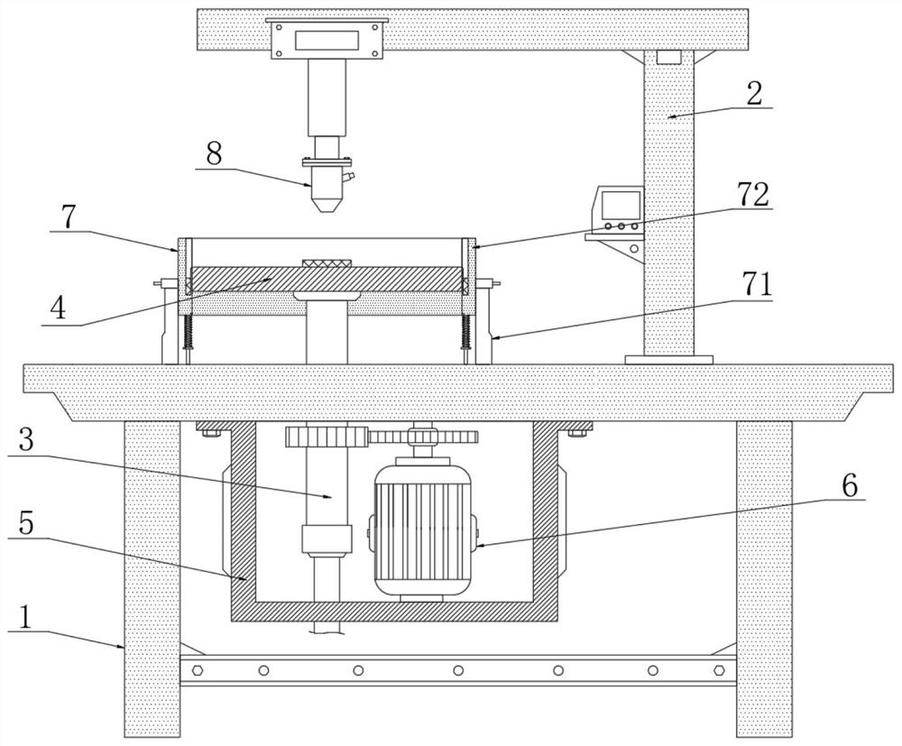
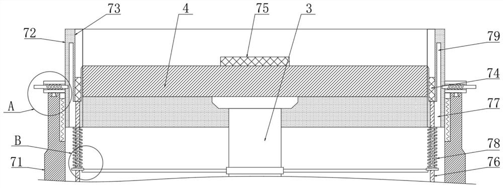
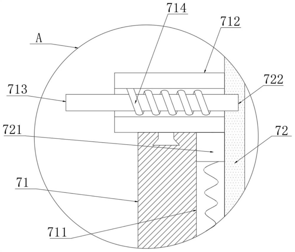
[0019] The present invention provides a technical solution: a wafer glue spraying mechanism based on chip processing, please refer to figure 1 , including workbench 1;

[0020] see figure 1 , the outer wall on the right side of the top of the workbench 1 is fixedly installed with a frame 2, the inner wall on the top of the frame 2 is provided with a hydraulic cylinder, and the hydraulic rod at the bottom of the hydraulic cylinder is fixedly connected to the n...


PUM


Abstract

The invention discloses a wafer glue spraying mechanism based on chip processing in the technical field of chip processing. The wafer glue spraying mechanism comprises a workbench, a rack is fixedly installed on the outer wall of the right side of the top of the workbench, a hydraulic cylinder is arranged on the inner wall of the top of the rack, a hydraulic rod at the bottom of the hydraulic cylinder is fixedly connected with a nozzle, the outer wall of the left side of the top of the workbench is rotationally connected with a rotating pipe, the bottom end of the rotating pipe is fixedly connected with an air pump through a pipeline, the rotating pipe is rotationally connected with the pipeline, the outer wall of a supporting table is sleeved with a shielding device, the outer side of thesupporting table is shielded through a shielding cover of the shielding device, so that photoresist does not fall onto the workbench due to rotation, the periphery of the equipment is protected; anda collecting tank is used for collecting redundant photoresist, so that the photoresist is prevented from being accumulated on the edge of the top wall of the wafer to cause non-uniform coating of thephotoresist.

Description

technical field [0001] The invention relates to the technical field of chip processing, in particular to a wafer glue spraying mechanism based on chip processing. Background technique [0002] A wafer is a silicon wafer for making silicon semiconductor integrated circuits. When the wafer is being processed, a layer of photoresist needs to be evenly sprayed on the surface of the wafer. Generally, the photoresist is dropped on the surface of the wafer through glue spraying equipment. Then the wafer is rotated by the external equipment, and under the action of the centrifugal force generated by the rotation and the surface tension of the photoresist, a photoresist film with uniform thickness is formed on the surface of the wafer. However, during the process of rotating the photoresist, Because the photoresist will flow, the photoresist will diffuse to the outside of the wafer, causing part of the photoresist to flow out from the wafer surface and fall on the equipment, causing ...

Claims


Application Information

Patent Timeline
IPC IPC(8): B05C5/00B05C11/08B05C11/10B05C15/00B05C13/02G03F7/16
CPCB05C5/002B05C11/08B05C11/1039B05C15/00B05C13/02G03F7/162
Inventor 巩铁凡
Owner 芯钛科半导体设备(上海)有限公司
Why Eureka
Eureka Blog
Learn More