A superjunction device and its terminal

A device and terminal technology, applied in the field of super junction devices and their terminals, can solve the problems of unable to change the distribution of net charge, unable to suppress electric field concentration, etc., to achieve the effect of optimizing electric field distribution, suppressing electric field peaks, and improving withstand voltage

Active Publication Date: 2021-12-28
ZHEJIANG UNIV
View PDF11 Cites 0 Cited by
  • Summary
  • Abstract
  • Description
  • Claims
  • Application Information

AI Technical Summary

Problems solved by technology

Because by reducing the cell size of the terminal region, the distribution of the net charge cannot be changed, and the electric field concentration phenomenon caused by the cylindrical junction in the terminal region cannot be suppressed.

Method used


Image

  • A superjunction device and its terminal
  • A superjunction device and its terminal
  • A superjunction device and its terminal

Examples


Embodiment Construction

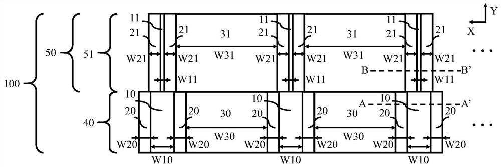
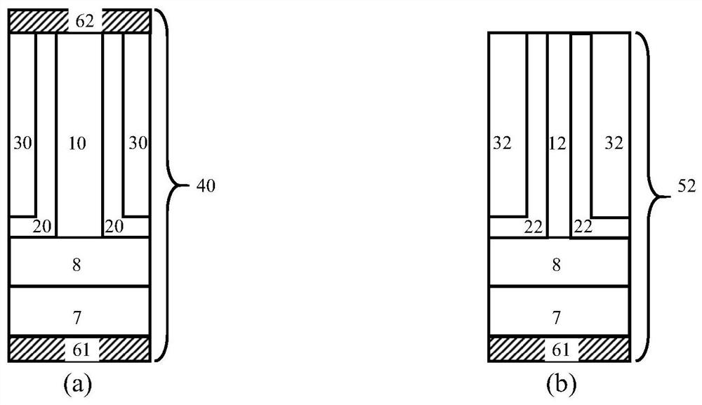
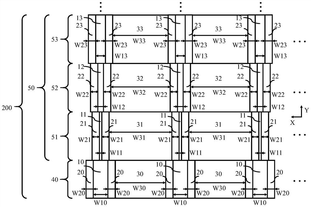
[0014] Specific embodiments of the present invention will be described in detail below in conjunction with the accompanying drawings. It should be noted that the embodiments described here are only for illustration, not for limiting the present invention. In the following description, numerous specific details are set forth in order to provide a thorough understanding of the present invention. However, it will be understood by one of ordinary skill in the art that these specific details are not required to practice the present invention. Additionally, in some embodiments, well-known structures, materials, or methods are not described in detail to avoid obscuring the present invention.

[0015] Throughout this specification, reference to "one embodiment," "an embodiment," "an example," or "example" means that a particular feature, structure, or characteristic described in connection with the embodiment or example is included in the present invention. In at least one embodiment...


PUM


Abstract

The invention discloses a semiconductor device and its terminal. The semiconductor device includes an active area and a terminal area. The semiconductor device includes a first column area, a second column area and a first dielectric column area located in the active area. and a first termination within the termination region, the first termination comprising a third stud region, a fourth stud region and a second dielectric stud region, wherein both the first stud region and the third stud region have a first doping type, Both the second column region and the fourth column region have the second doping type, the width of the third column region is smaller than the width of the first column region, the width of the fourth column region is greater than or equal to the width of the second column region, and the width of the second dielectric column region is greater than Or equal to the width of the first dielectric stud region. The structure of the present invention modulates the spatial distribution of negative charges in the terminal region on the basis of realizing negative charges in the terminal region during blocking, realizes a more uniform electric field distribution in the terminal region, and finally improves the withstand voltage of the device terminal.

Description

technical field [0001] The invention relates to a semiconductor device, in particular to a super junction device and its terminal. Background technique [0002] In recent years, more and more attention has been paid to energy saving and emission reduction in the world, which puts forward higher requirements for loss control and efficiency improvement of large power electronic equipment. As an important part of power electronic equipment, semiconductor power devices have received extensive attention from the industry. [0003] Breakdown voltage and specific on-resistance are important performance indicators of semiconductor power devices. With the advancement of device technology, power devices are gradually approaching their performance limits. In order to further improve device performance, increase breakdown voltage, and reduce specific on-resistance, super-junction structures have been proposed and widely used in power devices. The terminal protection structure outside...

Claims


Application Information

Patent Timeline
Patent Type & Authority Patents(China)
IPC IPC(8): H01L29/06
CPCH01L29/0634H01L29/0684
Inventor 盛况王珩宇郭清任娜王策
Owner ZHEJIANG UNIV
Why Eureka
Try Eureka