

Display panel, manufacturing method thereof and display device
A technology for display panels and encapsulation layers, which is used in the manufacture of semiconductor/solid-state devices, diodes, organic semiconductor devices, etc., and can solve the problems of color shift, low color purity of light, and poor display effect of display panels.
- Summary
- Abstract
- Description
- Claims
- Application Information
AI Technical Summary
Problems solved by technology
Method used
Image

Examples
Embodiment 1
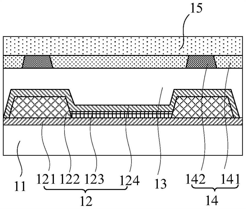
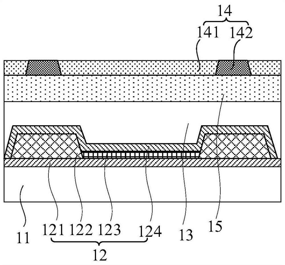
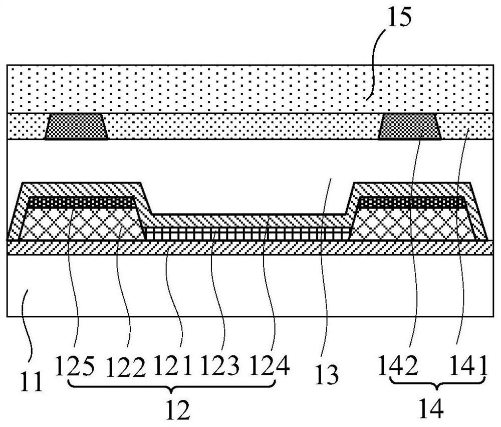
[0052] refer to figure 1 , showing a schematic structural diagram of a display panel according to an embodiment of the present invention, figure 2 shows a schematic structural diagram of another display panel according to an embodiment of the present invention, image 3 A schematic structural diagram of another display panel according to an embodiment of the present invention is shown.
[0053] An embodiment of the present invention provides a display panel, including: a driving backplane 11, a light emitting device layer 12 disposed on the driving backplane 11, and an encapsulation layer 13 respectively disposed on the side of the light emitting device layer 12 away from the driving backplane 11 , color filter layer 14 and light-absorbing layer 15; wherein, the light-absorbing layer 15 is configured to absorb light of a specific wavelength in the light emitted by the external ambient light and the light-emitting device layer 12; the specific wavelength includes red light ba...
Embodiment 2
[0102] refer to Figure 5 , which shows a flow chart of a method for manufacturing a display panel according to an embodiment of the present invention, which may specifically include the following steps:
[0103] Step 501, providing a driving backplane.
[0104] In the embodiment of the present invention, the driving backplane 11 for driving the light emitting device layer 12 to emit light is first fabricated.
[0105] Specifically, an active layer is formed on the substrate by a patterning process, a gate insulating layer covering the active layer and the substrate is formed, a gate layer is formed on the gate insulating layer by a patterning process, and a covering gate layer and a gate insulating layer are formed. The interlayer dielectric layer, then, form the first via hole and the second via hole through the interlayer dielectric layer and the gate insulating layer, then, adopt patterning process on the interlayer dielectric layer to form the source-drain electrode laye...
Embodiment 3
[0139] refer to Image 6 , shows a schematic structural diagram of a display device according to an embodiment of the present invention.
[0140] An embodiment of the present invention provides a display device, including a cover plate 20 and the above-mentioned display panel; the cover plate 20 is disposed on a light-emitting surface of the display panel.
[0141] Wherein, the cover plate 20 may be a glass cover plate for protecting the display panel. When the encapsulation layer 13 , the color filter layer 14 and the light absorbing layer 15 are sequentially arranged on the side of the light emitting device layer 12 away from the driving backplane 11 , the cover plate 20 is arranged on the side of the light absorbing layer 15 away from the color filter layer 14 ; When the encapsulation layer 13 , the light absorbing layer 15 and the color filter layer 14 are sequentially arranged on the side of the light emitting device layer 12 away from the driving backplane 11 , the cove...
PUM
 Abstract
Description
Claims
Application Information