
Semiconductor laser

a laser and semiconductor technology, applied in the field of semiconductor lasers, can solve the problems of increasing relative intensity noise, limiting high-power operation, and burning holes and kinking, and achieve the effect of reducing the variation of oscillation wavelength

Inactive Publication Date: 2008-07-08
MITSUBISHI ELECTRIC CORP
View PDF6 Cites 2 Cited by
  • Summary
  • Abstract
  • Description
  • Claims
  • Application Information

AI Technical Summary

Benefits of technology

The present invention provides a semiconductor laser that can achieve good high-speed response characteristics. The laser has a relaxation oscillation frequency that does not vary much in the axial direction of the resonator, even if the photon density distribution within the resonator is not uniform. This is achieved by reducing the optical confinement factor in a specific portion of the diffraction grating layer in an optical waveguide direction. The invention also provides a semiconductor laser that can achieve high-speed response characteristics by reducing the thickness of a high refractive index layer or by varying the pitch of the diffraction grating layer in the axial direction of the resonator. These features prevent distortion of the modulated light waveform and allow the laser to achieve good high-speed response characteristics.

Problems solved by technology

This semiconductor laser has a problem in that if the carrier density of the active layer is increased to achieve high output power, the density varies in a lateral direction, these causing hole burning and kinking and hence limiting high-power operation.
This semiconductor laser device has a problem in that the distance between the fiber grating and the semiconductor light-emitting element is large, resulting in increased relative intensity noise due to resonance between the fiber grating and the light reflective film.
This makes it difficult to achieve stable Raman amplification.
As a result, the response speed within the resonator varies in the axial direction, that is, the resonator has a non-uniform response speed distribution in the axial direction.
Therefore, when a semiconductor laser having a non-uniform photon density distribution is subjected to direct modulation operation at high speed (e.g., 10 Gbps), the problem of distortion of the modulated light waveform, etc. arises.

Method used


Image

  • Semiconductor laser
  • Semiconductor laser
  • Semiconductor laser

Examples


first embodiment

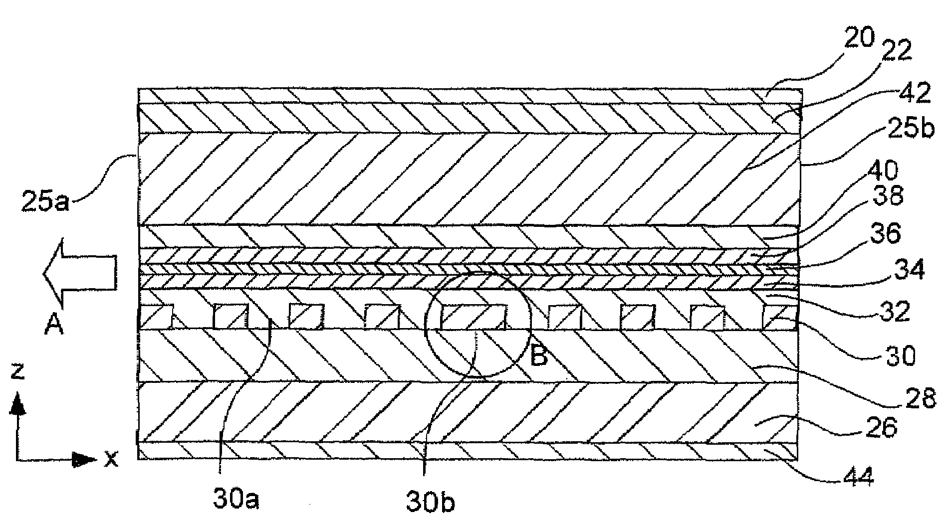
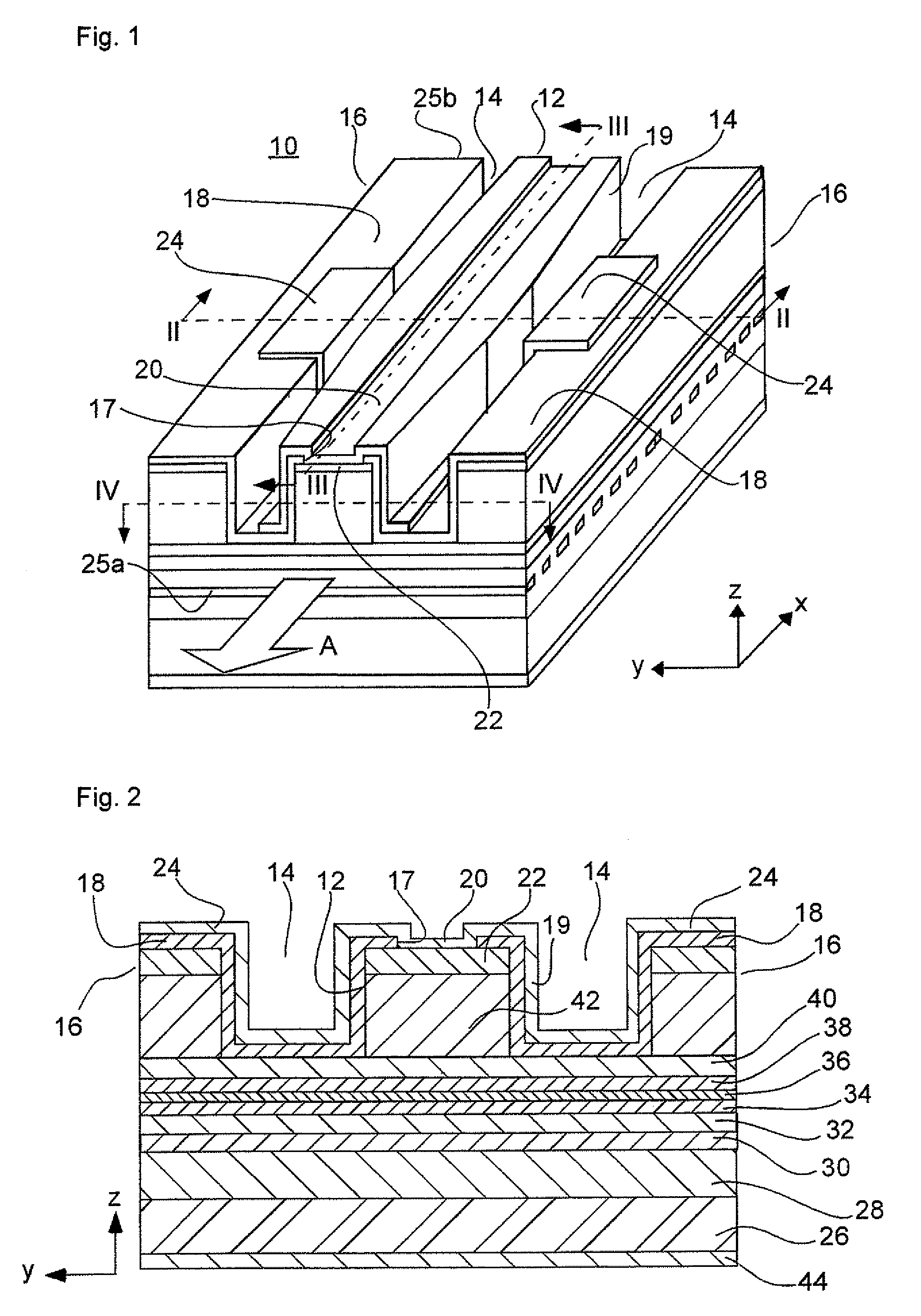
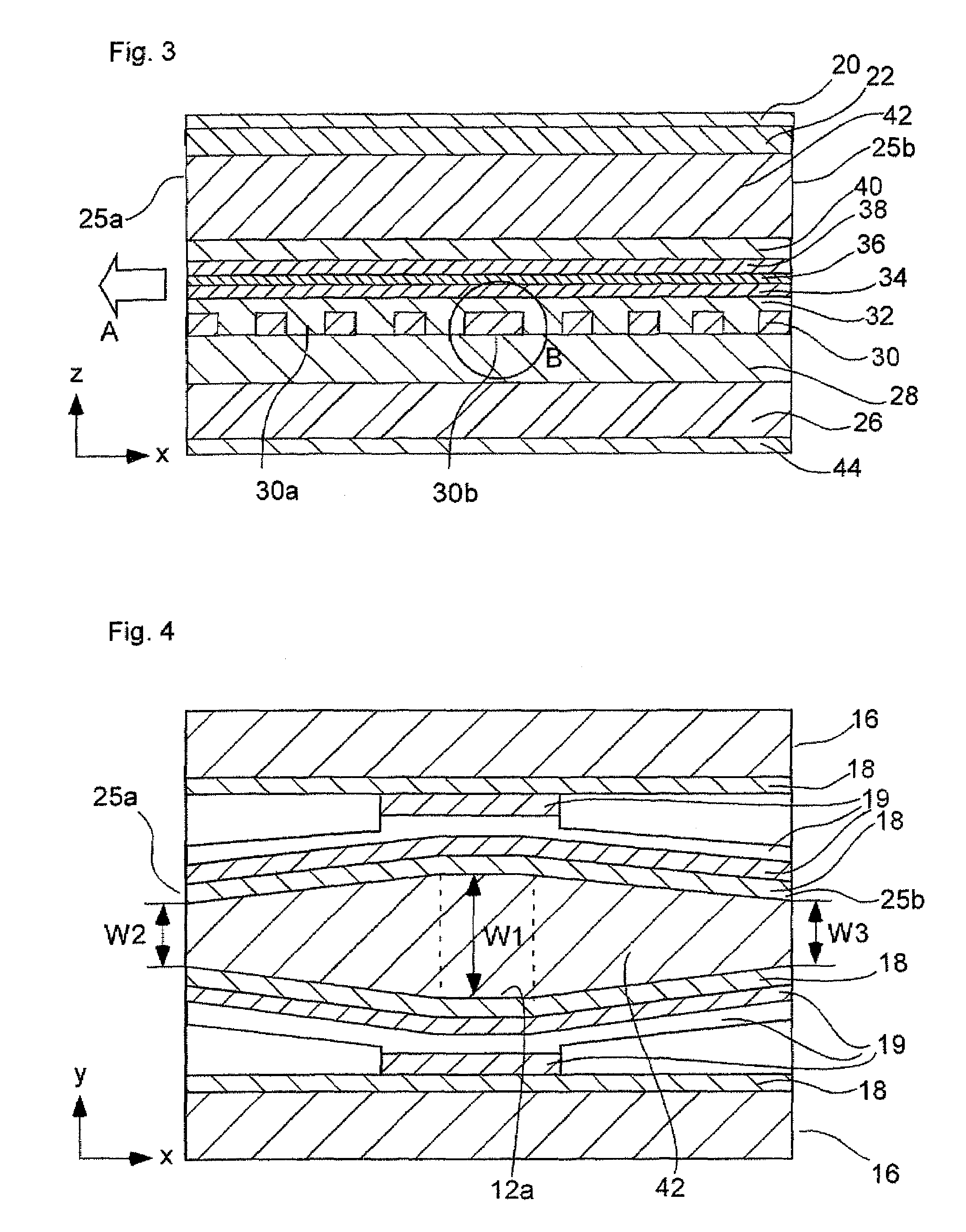
[0048]FIG. 1 is a perspective view of a semiconductor laser according to one embodiment of the present invention; FIG. 2 is a cross-sectional view of the semiconductor laser taken along line II-II of FIG. 1; FIG. 3 is a cross-sectional view of the semiconductor laser taken along line III-III of FIG. 1; and FIG. 4 is a cross-sectional view of the semiconductor laser taken along line IV-IV of FIG. 1. It should be noted that in these figures, like numerals are used to denote like or corresponding components.

[0049]Referring to FIG. 1, the semiconductor laser of the present embodiment is a waveguide ridge type DFB-LD 10 having an oscillation wavelength of 1.3 μm and a resonator length L of approximately 100-250 μm, for example.

[0050]A waveguide ridge 12 at the center portion of the DFB-LD 10 extends in the laser light emission direction. Two electrode pad bases 16 are disposed on respective sides of the waveguide ridge 12. A separation groove 14 is disposed between each electrode pad bas...

second embodiment

[0087]FIG. 10 is a perspective view of a semiconductor laser according to one embodiment of the present invention; FIG. 11 is a cross-sectional view of the semiconductor laser taken along line XI-XI of FIG. 10; FIG. 12 is a cross-sectional view of the semiconductor laser taken along line XII-XII of FIG. 10; and FIG. 13 is a cross-sectional view of the semiconductor laser taken along line XIII-XIII of FIG. 10.

[0088]Referring to FIG. 10, the semiconductor laser of the second embodiment of the present invention is a buried heterostructure DFB-LD 50 having an oscillation wavelength of 1.3 μm and a resonator length L of approximately 100-250 μm, for example.

[0089]A buried heterostructure 52 at the center portion of the DFB-LD 50 extends in the laser light emission direction. In FIG. 10, arrow A represents the laser light, and the direction of arrow A is the emission direction of the light. Two electrode pad bases 16 are disposed on respective sides of the buried heterostructure 52. A sep...

third embodiment

[0118]FIG. 15 is a cross-sectional view of a semiconductor laser according to one embodiment of the present invention.

[0119]The semiconductor laser shown in FIG. 15 is a waveguide ridge type DFB-LD 70 similar to the DFB-LD 10 of the first embodiment. Specifically, the DFB-LD 70 has the same configuration as the DFB-LD 10 except that the diffraction grating layer 30 of the DFB-LD 70 does not include the phase shift structure 30b. Therefore, a cross-sectional view of the DFB-LD 70 taken along a plane perpendicular to the resonator axis is similar to the cross-sectional view shown in FIG. 2.

[0120]Further, the cross-sectional view of the DFB-LD 70, specifically, the second p-cladding layer 42 shown in FIG. 15 corresponds to that shown in FIG. 4 and is taken along a plane parallel to the layers of the waveguide ridge 12, that is, parallel to the main surface of the substrate 26, showing how the width of the waveguide ridge 12 vary in the axial direction of the resonator.

[0121]In the DFB-...


PUM


Abstract

A semiconductor laser according to the present invention comprises: a substrate; an n-cladding layer disposed on the substrate; an active layer disposed on the n-cladding layer; a p-cladding layer disposed on the active layer and forming a waveguide ridge; and a diffraction grating layer disposed between the active layer and the n-cladding layer or the p-cladding layer and including a phase shift structure in a part of the diffraction grating layer in an optical waveguide direction. The width of the p-cladding layer is increased in a portion corresponding to the phase shift structure of the diffraction grating layer.

Description

BACKGROUND OF THE INVENTION[0001]1. Field of the Invention[0002]The present invention relates to a semiconductor laser, and more particularly to a distributed feedback semiconductor laser used as a light source for optical fiber communications, etc.[0003]2. Description of the Related Art[0004]In recent years, as broadband communications and public telecommunication networks using optical fibers have become widely used, there has been an increasing need to transmit a large amount of information at low cost. To meet such a need, it is necessary to increase the amount of information that can be transmitted per unit time, that is, to increase the information transmission rate. Actually, the transmission rate has been progressively increased from 600 Mbps to 2.5 Gbps, to 10 Gbps.[0005]Such an increase in the transmission rate of optical communications devices has led to an expansion in the market for optical communications networks for use not only in trunk systems but in access systems ...

Claims


Application Information

Patent Timeline
Patent Type & Authority Patents(United States)
IPC IPC(8): H01S5/00H01S5/12
CPCH01S5/12H01S5/1064H01S5/22H01S5/124H01S5/20H01S5/1225
Inventor TAKAGI, KAZUHISA
Owner MITSUBISHI ELECTRIC CORP
Learn More