

Semiconductor laser
a semiconductor laser and laser technology, applied in semiconductor lasers, laser optical resonator construction, laser details, etc., can solve the problems of increasing relative intensity noise, limiting high-power operation, and kinking of holes, so as to reduce the variation of oscillation wavelength
- Summary
- Abstract
- Description
- Claims
- Application Information
AI Technical Summary
Benefits of technology
Problems solved by technology
Method used
Image

Examples
first embodiment
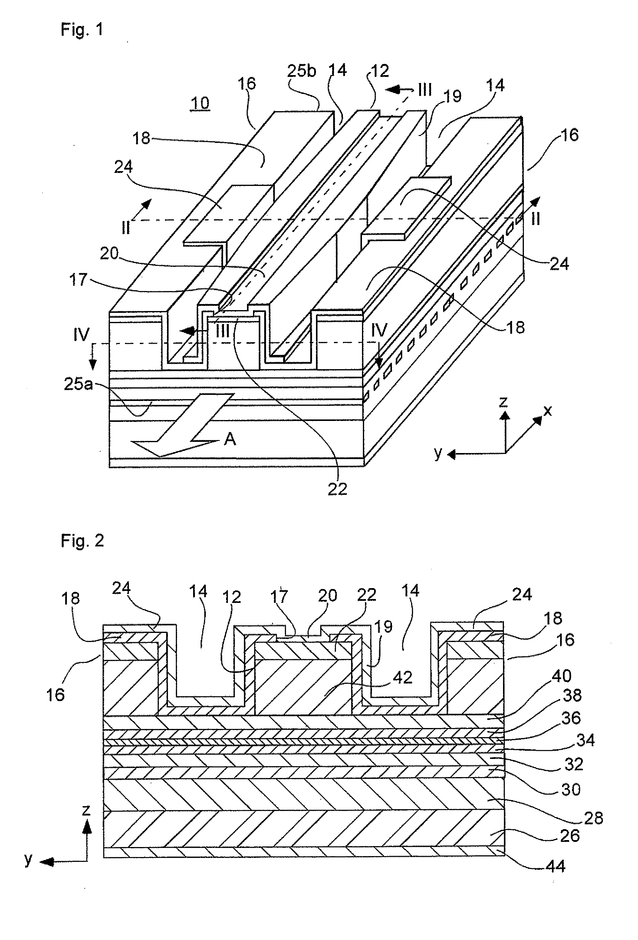
[0048]FIG. 1 is a perspective view of a semiconductor laser according to one embodiment of the present invention; FIG. 2 is a cross-sectional view of the semiconductor laser taken along line II-II of FIG. 1; FIG. 3 is a cross-sectional view of the semiconductor laser taken along line III-III of FIG. 1; and FIG. 4 is a cross-sectional view of the semiconductor laser taken along line IV-IV of FIG. 1. It should be noted that in these figures, like numerals are used to denote like or corresponding components.
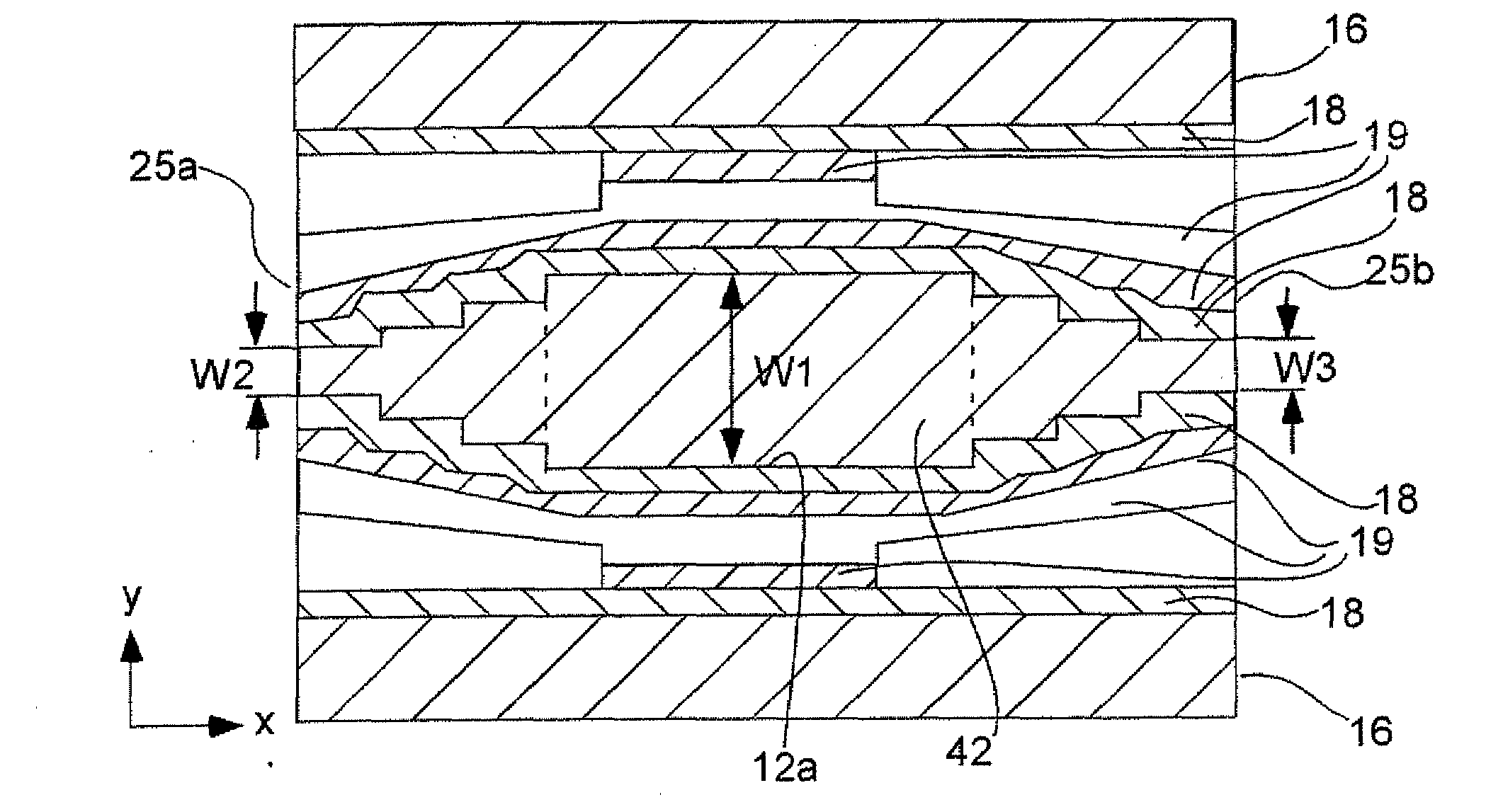
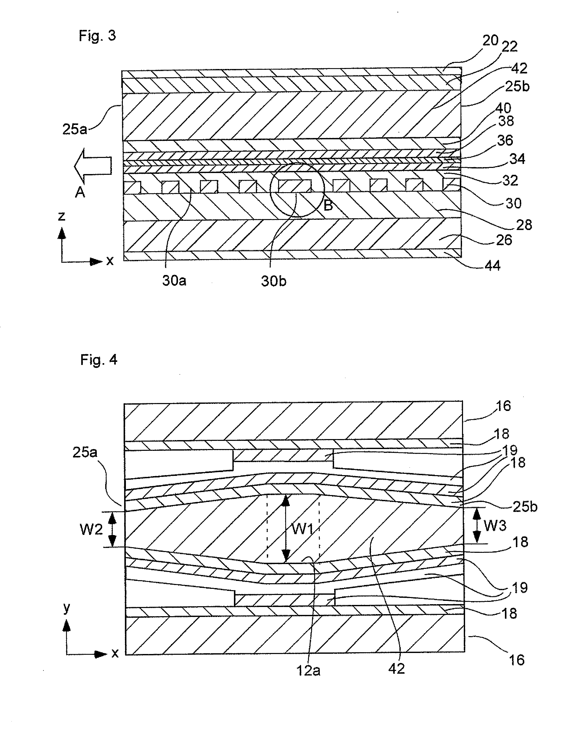
[0049]Referring to FIG. 1, the semiconductor laser of the present embodiment is a waveguide ridge type DFB-LD 10 having an oscillation wavelength of 1.3 μm and a resonator length L of approximately 100-250 μm, for example.
[0050]A waveguide ridge 12 at the center portion of the DFB-LD 10 extends in the laser light emission direction. Two electrode pad bases 16 are disposed on respective sides of the waveguide ridge 12. A separation groove 14 is disposed between each electrode pad bas...
second embodiment
[0087]FIG. 10 is a perspective view of a semiconductor laser according to one embodiment of the present invention; FIG. 11 is a cross-sectional view of the semiconductor laser taken along line XI-XI of FIG. 10; FIG. 12 is a cross-sectional view of the semiconductor laser taken along line XII-XII of FIG. 10; and FIG. 13 is a cross-sectional view of the semiconductor laser taken along line XIII-XIII of FIG. 10.
[0088]Referring to FIG. 10, the semiconductor laser of the second embodiment of the present invention is a buried heterostructure DFB-LD 50 having an oscillation wavelength of 1.3 μm and a resonator length L of approximately 100-250 μm, for example.
[0089]A buried heterostructure 52 at the center portion of the DFB-LD 50 extends in the laser light emission direction. In FIG. 10, arrow A represents the laser light, and the direction of arrow A is the emission direction of the light. Two electrode pad bases 16 are disposed on respective sides of the buried heterostructure 52. A sep...
third embodiment
[0118]FIG. 15 is a cross-sectional view of a semiconductor laser according to one embodiment of the present invention.
[0119]The semiconductor laser shown in FIG. 15 is a waveguide ridge type DFB-LD 70 similar to the DFB-LD 10 of the first embodiment. Specifically, the DFB-LD 70 has the same configuration as the DFB-LD 10 except that the diffraction grating layer 30 of the DFB-LD 70 does not include the phase shift structure 30b. Therefore, a cross-sectional view of the DFB-LD 70 taken along a plane perpendicular to the resonator axis is similar to the cross-sectional view shown in FIG. 2.
[0120]Further, the cross-sectional view of the DFB-LD 70, specifically, the second p-cladding layer 42 shown in FIG. 15 corresponds to that shown in FIG. 4 and is taken along a plane parallel to the layers of the waveguide ridge 12, that is, parallel to the main surface of the substrate 26, showing how the width of the waveguide ridge 12 vary in the axial direction of the resonator.
[0121]In the DFB-...
PUM
 Abstract
Description
Claims
Application Information