Vertical power transistor and method for producing the vertical power transistor

A technology of power transistors and semiconductors, applied in the manufacture of semiconductor/solid-state devices, semiconductor devices, electrical components, etc., can solve the problems of changing field scale, semiconductor crystal damage, high cost, etc.

Pending Publication Date: 2021-02-26
ROBERT BOSCH GMBH
View PDF0 Cites 0 Cited by
  • Summary
  • Abstract
  • Description
  • Claims
  • Application Information

AI Technical Summary

Problems solved by technology

[0006] Disadvantages here are that high energy must be used for deep implantation, thereby causing high costs, leading to severe damage to the semiconductor crystal, and lateral ion scattering changing the field scale (Pitchmaβ)

Method used


Image

  • Vertical power transistor and method for producing the vertical power transistor
  • Vertical power transistor and method for producing the vertical power transistor
  • Vertical power transistor and method for producing the vertical power transistor

Examples


Embodiment Construction

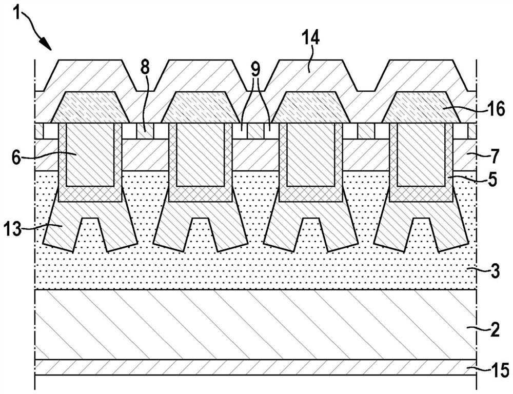
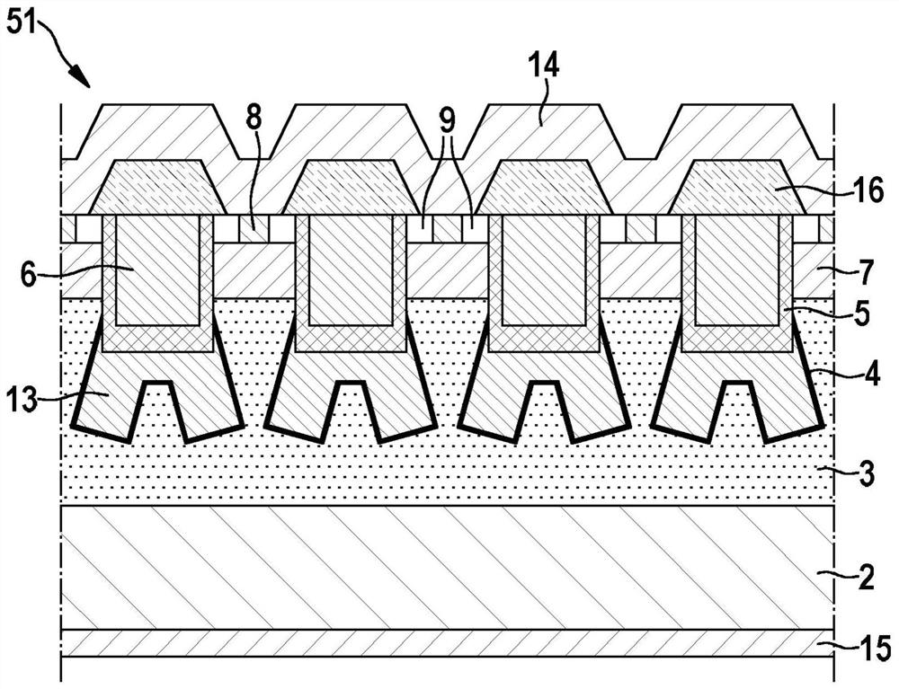
[0032] figure 1 A vertical power transistor 1 is shown having a semiconductor substrate 2 on whose front side at least one epitaxial layer 3 is arranged. The vertical power transistor 1 is, for example, a Metal Oxide Semiconductor Field Effect Transistor (Mosfet). The semiconductor substrate 2 comprises a first semiconductor material, for example silicon carbide, in particular 4H—SiC, wherein the epitaxial layer 3 is n-doped.

[0033] Arranged on the epitaxial layer 3 is a second layer 7 which functions as a channel region or body region. Arranged on the second layer 7 is a third layer comprising a body junction region 8 and a source region 9 . Arranged on the rear side of the semiconductor substrate 2 is a second metal layer 15 which functions as a drain metallization. The vertical power transistor 1 has a trench structure, that is, a plurality or a plurality of trenches. The trenches have a depth of 0.5 μm to 14 μm and a pitch of 0.2 μm to 10 μm measured at the respectiv...


PUM


Abstract

The invention relates to a vertical power transistor (1) having a semiconductor substrate (2) which is composed of a first semiconductor material and has at least one epitaxial layer (3), wherein a trench structure extends from a surface of the semiconductor substrate (2) into the interior of the at least one epitaxial layer (3), characterized in that the trench structure has first regions (13) which each extend from a trench bottom up to a specific height of the respective trench, wherein: the first regions (13) comprise first sub-regions, each having a first depth (t1) and a first width (w1); the first sub-regions extend substantially perpendicularly to the surface of the semiconductor substrate (2); the first regions (13) comprise second sub-regions, each having a second depth and a second width (w2); the second sub-regions have a first angle of inclination relative to the surface of the semiconductor substrate (2); the first regions (13) comprise third sub-regions, each having a third depth and a third width; the third sub-regions have a second angle of inclination relative to the surface of the semiconductor substrate (2); and the first regions (13) are electrically conductively connected to a source terminal.

Description

technical field [0001] The present invention relates to a vertical power transistor with a specifically shaped trench structure and a method for manufacturing a vertical power transistor. Background technique [0002] In vertical power transistors, the shielding of the gate oxide against high field strengths is problematic when a high positive voltage is applied between drain and source in blocking operation and in the event of a short circuit. Furthermore, the limitation of the short-circuit current is difficult. [0003] Various possibilities for shielding the gate oxide are known from the prior art. One possibility is to embed or excavate p-doped regions in the epitaxial layer below the trench structure of the power transistor. The p-doped region is electrically connected to the source region of the power transistor. Due to the position of the p-doped region below the MIS head, the p-doped region shields the MIS head from high field strengths and significantly contribu...

Claims


Application Information

Patent Timeline
Patent Type & Authority Applications(China)
IPC IPC(8): H01L29/165H01L29/423H01L29/78H01L21/336H01L29/06
CPCH01L29/0623H01L29/1608H01L29/165H01L29/4236H01L29/66068H01L29/66734H01L29/7813
Inventor H·鲍托尔夫A·格拉赫S·施魏格尔
Owner ROBERT BOSCH GMBH
Why Eureka
Try Eureka