Display panel, manufacturing method thereof and display device
A display panel and display chip technology, applied in electrical components, electrical solid devices, circuits, etc., can solve problems such as poor user experience, achieve the effects of reducing black border area, prolonging service life, and improving user experience
- Summary
- Abstract
- Description
- Claims
- Application Information
AI Technical Summary
Problems solved by technology
Method used
Image
Examples
Embodiment 1
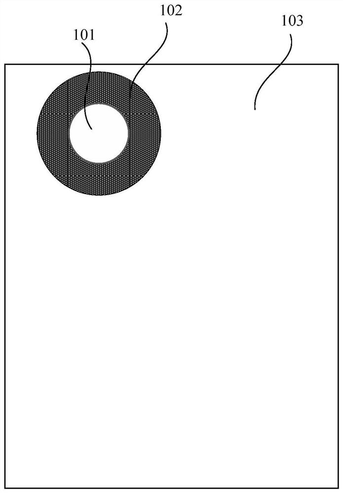
[0039] figure 1 It is a top view of a display panel disclosed in Embodiment 1 of the present invention, such as figure 1 As shown, the display panel has a preset hole 101 for setting a camera module, an area 102 between the preset hole and the effective display area, and an effective display area 103 . figure 1 The shaded pattern filled area in is the area 102 between the preset hole and the effective display area.
[0040] The devices provided in the above-mentioned camera module include but are not limited to at least one of a distance sensor, a light sensor, a camera and an infrared sensor. The preset hole 101 in this embodiment is circular, which is not limited in the present invention. The preset hole 101 may also be a quadrilateral or other shapes, which can be set by those skilled in the art as required.
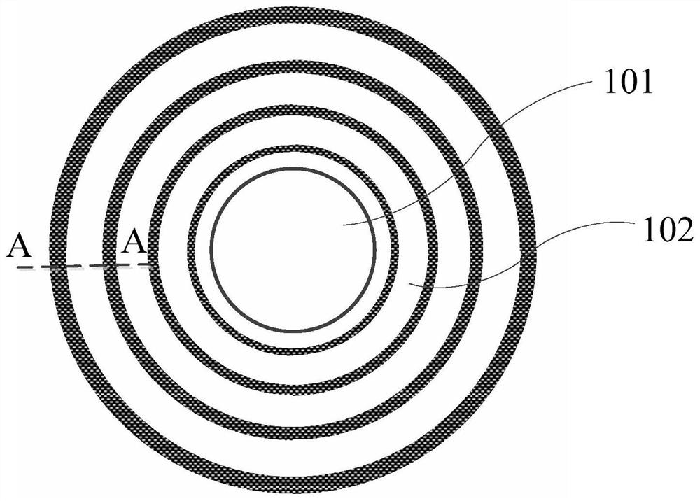
[0041] figure 2 for figure 1A partially enlarged schematic diagram of the area 102 between the preset hole and the effective display area of the middle display...
Embodiment 2
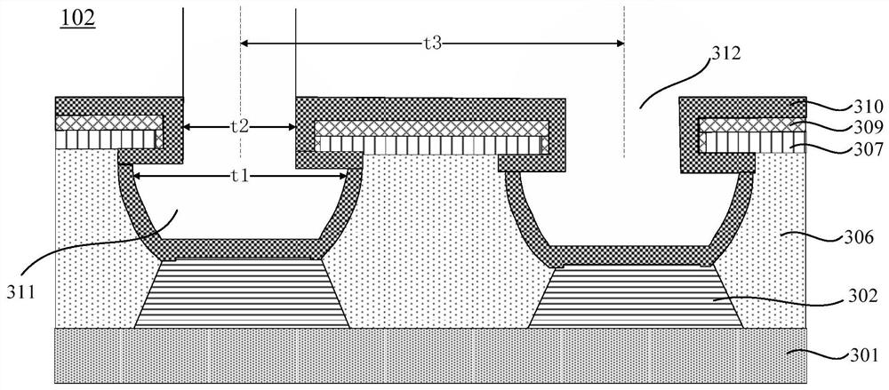
[0051] Figure 4 A cross-sectional view along the A-A direction of the area between the preset hole 101 and the effective display area 103 disclosed for the second embodiment, as shown in Figure 4 As shown, on the basis of Embodiment 1, the display panel further includes:
[0052] The second buffer layer 303, the second buffer layer 303 is formed on the side of the barrier layer 302 away from the substrate 301 and covers the substrate 301, the second buffer layer 303 forms the organic film group on the side away from the barrier layer 302 306, and the encapsulation layer 310 covers the side walls of the second isolation channel 312, the side walls of the first isolation channel 311, and the surface of the second buffer layer 303 (such as Figure 4 shown). The material of the second buffer layer 303 is an inorganic material, specifically silicon oxide, silicon nitride, silicon oxynitride, aluminum oxide or titanium oxide. The present invention does not specifically limit th...
PUM
 Abstract
Description
Claims
Application Information


