Auxiliary chip design method for reducing simulation time

A technology of auxiliary chips and design methods, applied in computer-aided design, CAD circuit design, calculation, etc., can solve the problems of long simulation time, difficult schematic and layout adjustment, etc., to reduce simulation time, speed up, and reduce cost. effect of time

Active Publication Date: 2021-03-16
SUZHOU BATELAB MICROELECTRONICS
View PDF3 Cites 4 Cited by
  • Summary
  • Abstract
  • Description
  • Claims
  • Application Information

AI Technical Summary

Problems solved by technology

[0004] In order to overcome the deficiencies of the above-mentioned prior art, the object of the present invention is to propose an auxiliary chip desi...

Method used


Image

  • Auxiliary chip design method for reducing simulation time
  • Auxiliary chip design method for reducing simulation time
  • Auxiliary chip design method for reducing simulation time

Examples


Embodiment Construction

[0025] The specific embodiments of the present invention will be described in further detail below in conjunction with the accompanying drawings, so as to make the technical solutions of the present invention easier to understand and grasp, so as to make a clearer definition of the protection scope of the present invention.

[0026] Aiming at the existing deficiencies, the designer of the present invention innovatively proposes an auxiliary chip design method based on the long-term experience in chip design such as analog integrated circuits, so as to optimize the chip design process. The main energy is to design some circuit modules with special functions required by the chip to speed up the chip design.

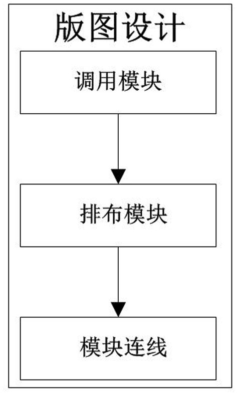
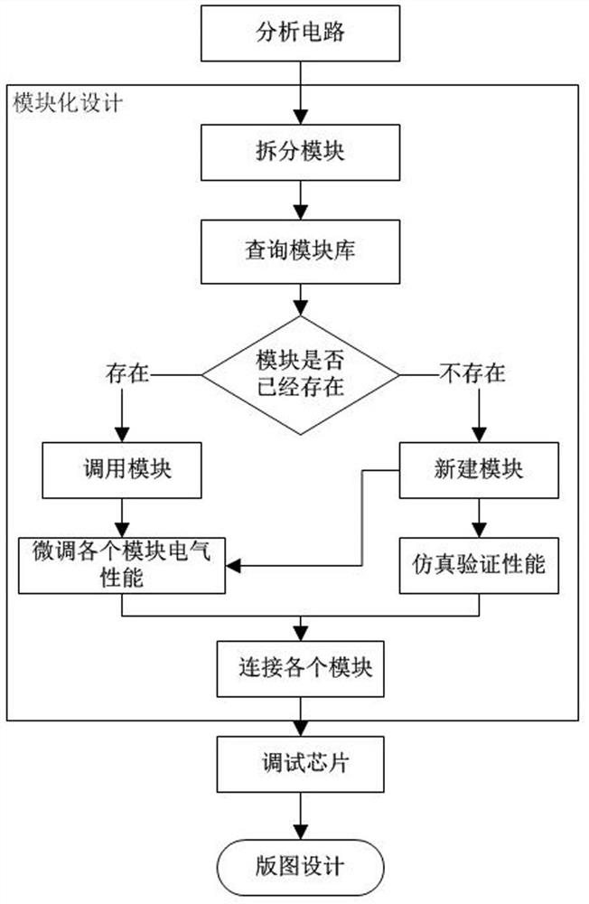
[0027] like figure 2 It can be seen from the schematic flow chart shown that the technical overview of the auxiliary chip design of the present invention mainly includes the following steps: S1. Establish a standard component library, classify various ready-made and verifi...


PUM


Abstract

The invention discloses an auxiliary chip design method for reducing simulation time. The method comprises the following steps: firstly, establishing a standard element library; establishing a reference model of the analog integrated circuit according to function classification, wherein the reference model comprises element library information of automatic calling and combined connection, a parameter filling space and a part of blank modules needing to be manually designed; selecting a reference model in a development tool according to required functions, filling in parameters, generating a schematic diagram top layer circuit, each module sub-circuit and a form required by module verification, and importing the schematic diagram top layer circuit, each module sub-circuit and the form intoa schematic diagram editor to complete schematic diagram design; and finally, importing a layout design tool, calling the corresponding layout and drawing layout in the standard element library, and verifying, integrating and completely drawing. By applying the method provided by the invention, the consumed time caused by layout rearrangement due to schematic diagram adjustment can be reduced, meanwhile, the simulation time required by most module function verification is also reduced, and the chip design speed is greatly increased.

Description

technical field [0001] The invention relates to a semiconductor chip design method, in particular to an auxiliary chip design method for reducing simulation time in the design of an analog integrated circuit. Background technique [0002] like figure 1 As shown in the figure, in the current design of analog circuit chips, each functional module is drawn separately, and finally the wiring is placed uniformly to form a complete chip. The principle design part often creates a new circuit structure or modifies part of the parameters of the module due to the actual design requirements; The layout part needs to make the corresponding actual layout circuit according to the modification of the principle part. [0003] The parameters modified due to the schematic diagram part vary from person to person due to the personal experience of the principle designer. For example, in order to reduce the current of a branch in the circuit, the resistance of the branch can be increased, or th...

Claims


Application Information

Patent Timeline
IPC IPC(8): G06F30/398G06F30/31G06F115/02
CPCG06F30/31G06F30/398G06F2115/02
Inventor 李真
Owner SUZHOU BATELAB MICROELECTRONICS
Why Eureka
Try Eureka