A germanium silicon avalanche photodetector

An avalanche photoelectric and detector technology, applied in the field of detectors, can solve the problems of large dark current and low photoelectric conversion efficiency, and achieve the effect of reducing dark current and improving photoelectric conversion efficiency

Active Publication Date: 2022-06-28
JILIN UNIV
View PDF0 Cites 0 Cited by
  • Summary
  • Abstract
  • Description
  • Claims
  • Application Information

AI Technical Summary

Problems solved by technology

However, the research on Ge as a low-light detector-avalanche photodiode has just begun, and it has a series of problems such as large dark current and low photoelectric conversion efficiency.

Method used


Image

  • A germanium silicon avalanche photodetector
  • A germanium silicon avalanche photodetector
  • A germanium silicon avalanche photodetector

Examples


Embodiment Construction

[0071] The technical solutions in the embodiments of the present invention will be clearly and completely described below with reference to the accompanying drawings in the embodiments of the present invention. Obviously, the described embodiments are only a part of the embodiments of the present invention, but not all of the embodiments. Based on the embodiments of the present invention, all other embodiments obtained by those of ordinary skill in the art without creative efforts shall fall within the protection scope of the present invention.

[0072] In order to make the above objects, features and advantages of the present invention more clearly understood, the present invention will be described in further detail below with reference to the accompanying drawings and specific embodiments.

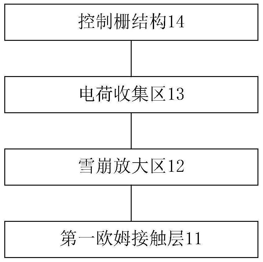
[0073] refer to figure 1 , figure 1 This is a schematic diagram of the principle of a germanium-silicon avalanche photodetector provided by an embodiment of the present invention.

[...


PUM


Abstract

The invention provides a germanium-silicon avalanche photodetector, comprising: an avalanche amplification region; a first ohmic contact layer and a charge collection region respectively in contact with the avalanche amplification region; a control gate structure connected to the charge collection region; Wherein, the control gate structure is used to control the barrier height of the charge collection region. That is to say, based on the control gate structure, the silicon germanium avalanche photodetector controls the barrier height of the charge collection region by adjusting the gate voltage, so that only the carrier accumulation potential energy in the dark current is higher than a certain potential barrier Only when it is allowed to pass through, the dark current of the germanium-silicon avalanche photodetector is reduced, and the photoelectric conversion efficiency is improved.

Description

technical field [0001] The present invention relates to the technical field of detectors, and more particularly, to a germanium-silicon avalanche photodetector. Background technique [0002] As a weak light detector, germanium-silicon avalanche photodiode (Avalanche Photo Diode, APD for short) has very important applications in many aspects such as optical communication, laser imaging and lidar. [0003] APDs in the visible light and near-infrared bands (300nm-1000nm) generally use Si materials, which are now very mature. APDs in the mid-infrared band (1.3μm-1.7μm) generally use III-V materials. The technology is very mature, but the cost is high and the uniformity is not good. It is very difficult to fabricate APD arrays in this band. In addition, silicon-based photonics has developed very rapidly in the past ten years. On the one hand, silicon-based photonics is fully compatible with silicon-based integrated circuits, and silicon-based optoelectronic chips will be very ch...

Claims


Application Information

Patent Timeline
Patent Type & Authority Patents(China)
IPC IPC(8): H01L31/107H01L31/0224H01L31/028H01L31/0352
CPCH01L31/107H01L31/022408H01L31/028H01L31/0352Y02E10/547
Inventor 宋俊峰王欣伟李雨轩刘晓斌李雪妍郜峰利
Owner JILIN UNIV
Why Eureka
Try Eureka