LED chip, LED chip packaging module and display device

A technology of LED chip and mesa structure, which is applied in the use of semiconductor devices, electrical components, and semiconductor lamps, etc., can solve reliability problems and other problems, and achieve the effect of improving reliability, improving reliability performance, and better performance.

Active Publication Date: 2021-03-19
XIAMEN SANAN OPTOELECTRONICS CO LTD
View PDF4 Cites 4 Cited by
  • Summary
  • Abstract
  • Description
  • Claims
  • Application Information

AI Technical Summary

Problems solved by technology

[0004] At present, one of the problems encountered in the development of LED chips in the direction of miniaturization is the reliability problem, that is, the industry is faced with the need to optimize the corresponding LED chip structure to improve product reliability.

Method used


Image

  • LED chip, LED chip packaging module and display device
  • LED chip, LED chip packaging module and display device
  • LED chip, LED chip packaging module and display device

Examples


Embodiment Construction

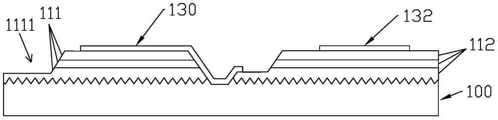
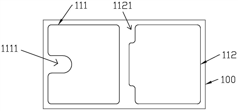
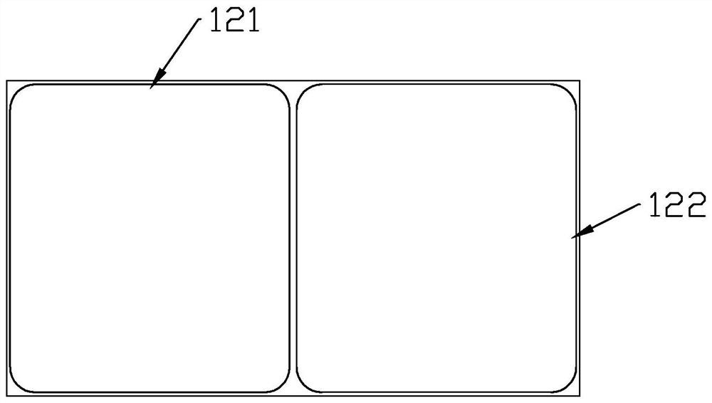
[0065] The present invention provides a new LED chip, LED chip packaging module and display device. For a clearer representation, the present invention will be described in detail below in conjunction with the accompanying drawings.

[0066] This manual adopts simplified labels for each structure, except Figure 12 and Figure 14 , the same structure is labeled only once on the cross-section and top-view projections, in order to show the structure more clearly.

[0067] An LED chip according to an embodiment of the present invention, please refer to Figure 1 to Figure 14 ,in Figure 14 It is a top-view projection schematic diagram of each structure of the entire LED chip, and shows a perspective structural schematic diagram of a solid line, that is, each structure is superimposed and displayed with a solid line.

[0068] Such as Figure 1 to Figure 14 As shown, the LED chip includes a substrate 100, a first mesa structure 111, a second mesa structure 112, and a cross curr...


PUM


Abstract

The invention discloses an LED chip, an LED chip packaging module and a display device. The LED chip comprises a substrate, a first mesa structure and a second mesa structure, at least one bridging current blocking block; bridging conductive blocks, the number of the bridging conductive blocks is the same as that of the bridging current stop blocks; a first conductive pad and a second conductive pad; wherein the overlooking projection of the bridging current stop block is provided with a head part and a tail part; the overlooking projection of the bridging conductive block is provided with a first contact part, a junction part and a second contact part; the junction part is located in the head part, and the first contact part is located in the tail part; the portion, not overlapped with the junction portion, of the head portion has a first width, the portion, not overlapped with the first contact portion, of the tail portion has a second width, and the first width is larger than the second width; reliability of the LED chip is improved.

Description

technical field [0001] The invention relates to the field of LEDs, in particular to an LED chip, an LED chip packaging module and a display device. Background technique [0002] LED (Light Emitting Diode) has the advantages of low cost, high luminous efficiency, energy saving and environmental protection, etc., and is widely used in lighting, visible light communication and light-emitting display and other scenarios. [0003] One of the development directions of LED is to develop towards miniaturization and miniaturization. After LED is shrunk, it forms an array with millimeter or even micron spacing, which can achieve ultra-high resolution, so that it can be more widely used in information display and other fields. Compared with liquid crystal display (LCD) and organic light-emitting display (OLED), LED has the advantages of long luminous life, high brightness, light and thin volume, low power consumption, and high pixel density. Display is one of the representatives of th...

Claims


Application Information

Patent Timeline
Patent Type & Authority Applications(China)
IPC IPC(8): H01L33/14H01L33/20H01L33/22H01L33/46H01L33/62H01L25/075
CPCH01L33/22H01L33/20H01L33/145H01L33/46H01L33/62H01L25/0753Y02B20/30
Inventor 刘士伟徐瑾刘可王水杰张中英曾合加
Owner XIAMEN SANAN OPTOELECTRONICS CO LTD
Why Eureka
Try Eureka