Modeling method for coaxial silicon through hole filled with a single-walled carbon nanotube

A single-walled carbon nanotube and carbon nanotube technology, applied in the field of electronics, can solve the problems of decreased electrical transmission performance, complicated calculation, insufficient circuit model accuracy, etc. Effect

Active Publication Date: 2021-03-23
XIDIAN UNIV
View PDF4 Cites 0 Cited by
  • Summary
  • Abstract
  • Description
  • Claims
  • Application Information

AI Technical Summary

Problems solved by technology

[0005] The purpose of the present invention is to address the shortcomings of the above-mentioned prior art, and propose a modeling method for filling single-walled carbon nanotube coaxial through-silicon vias, which is used to solve complex calculations, insufficient accuracy of circuit models, and sharp electrical transmission performance at high frequencies. falling problem
[0006] The idea of ​​realizing the object of the present invention is that in order to solve the problem of sharp decline in electrical transmission performance under high frequency conditions, a coaxial through-silicon via filled with single-walled carbon nanotubes is proposed, compared with the traditional coaxial via using copper as the transmission conductor Through-silicon vias, the present invention uses single-walled carbon nanotubes as transmission conductors, and at the same time, in order to improve the accuracy of the equivalent circuit model of coaxial silicon-through-holes filled with single-walled carbon nanotubes in integrated circuits, the present invention calculates according to the physical properties of carbon nanotubes The resistance parameters of carbon nanotubes, by extracting the resistance, inductance, capacitance and conductance parameters of the coaxial silicon vias filled with single-walled carbon nanotubes, the equivalent circuit model of the coaxial silicon vias is established

Method used


Image

  • Modeling method for coaxial silicon through hole filled with a single-walled carbon nanotube
  • Modeling method for coaxial silicon through hole filled with a single-walled carbon nanotube
  • Modeling method for coaxial silicon through hole filled with a single-walled carbon nanotube

Examples


Embodiment Construction

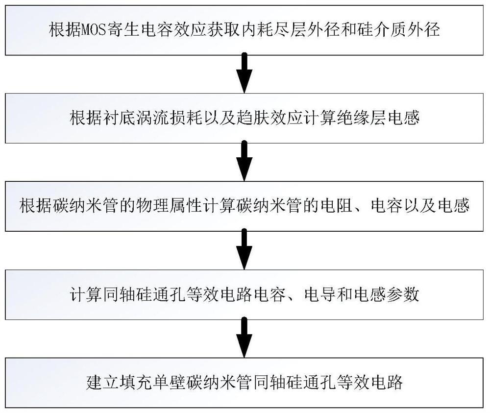
[0023] In order to make the object, technical solution and advantages of the present invention clearer, the present invention will be further described below in conjunction with the accompanying drawings and embodiments.

[0024] refer to figure 1 , further describe the steps realized by the present invention.

[0025] Step 1, calculate the outer diameter of the inner depletion layer and the outer diameter of the silicon dielectric according to the MOS parasitic capacitance effect.

[0026] The calculation of the outer diameter of the inner depletion layer and the outer diameter of the silicon medium includes:

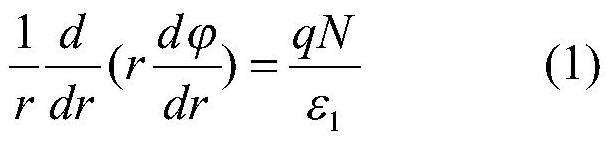
[0027] Set the expression and boundary conditions of the one-dimensional Poisson equation in the cylindrical coordinate system;

[0028] Integrate the expression according to the boundary conditions to obtain the outer diameter r of the inner depletion layer 1 and silicon dielectric outer diameter r 3 .

[0029] Step 2, calculate the inductance of the insulating l...


PUM


Abstract

The invention relates to a modeling method for a coaxial silicon through hole filled with a single-walled carbon nanotube. The modeling method comprises the following steps: calculating the outer diameter of a depletion layer and the outer diameter of a silicon medium in the coaxial silicon through hole filled with the single-walled carbon nanotube; calculating resistance, capacitance and inductance parameters of the carbon nanotubes according to the physical properties of the carbon nanotubes; calculating capacitance, conductivity and inductance parameters of the coaxial through silicon via equivalent circuit; and establishing an equivalent circuit model of the coaxial silicon through hole filled with the single-walled carbon nanotube. According to the coaxial silicon through hole filledwith the single-walled carbon nanotubes, loss is smaller under the condition of high-frequency signals, an established equivalent circuit model is more accurate, and meanwhile calculation is simple.

Description

technical field [0001] The invention belongs to the technical field of electronics, and further relates to a modeling method for filling coaxial through-silicon holes of single-walled carbon nanotubes in the technical field of electronic devices. The present invention can establish the equivalent circuit model of the through-silicon hole by extracting the resistance, inductance, capacitance and conductance parameters of the coaxial through-silicon hole filled with single-walled carbon nanotubes. Background technique [0002] Coaxial TSVs filled with single-walled carbon nanotubes are usually used for vertical interconnection between different layers of integrated circuits. Current passing through coaxial TSVs will generate resistance, inductance, and capacitance parasitic on the coaxial TSVs. As well as the conductance parameter, an equivalent circuit model is established through the resistance, inductance, capacitance and conductance parameters parasitic on the coaxial TSV ...

Claims


Application Information

Patent Timeline
IPC IPC(8): G06F30/337G06F30/39
CPCG06F30/337G06F30/39
Inventor 董刚谈豪朱思曈朱樟明杨银堂
Owner XIDIAN UNIV
Why Eureka
Try Eureka