Supercharge Your Innovation With Domain-Expert AI Agents!

Low-cost multi-chip high-speed high-bandwidth interconnection structure

An interconnect structure and multi-chip technology, applied in the direction of electrical components, electrical solid devices, circuits, etc., can solve the problems of high production cost and unsuitable for large-area integration, so as to improve computing power, reduce design difficulty and production cost Effect

Pending Publication Date: 2021-03-23
南京蓝洋智能科技有限公司
View PDF5 Cites 0 Cited by
  • Summary
  • Abstract
  • Description
  • Claims
  • Application Information

AI Technical Summary

Problems solved by technology

However, as Moore's Law comes to an end, the size of transistors is getting closer and closer to the limit, and the corresponding production costs are getting higher and higher
In addition, due to the material properties of silicon, silicon-based interposers are not naturally suitable for large-area integration

Method used


Image

  • Low-cost multi-chip high-speed high-bandwidth interconnection structure
  • Low-cost multi-chip high-speed high-bandwidth interconnection structure
  • Low-cost multi-chip high-speed high-bandwidth interconnection structure

Examples


Embodiment Construction

[0021] Embodiments of the present invention are described in detail below, examples of which are shown in the drawings, wherein the same or similar reference numerals designate the same or similar elements or elements having the same or similar functions throughout. The embodiments described below by referring to the figures are exemplary only for explaining the present invention and should not be construed as limiting the present invention.

[0022] Below in conjunction with accompanying drawing, technical scheme of the present invention is described in further detail:

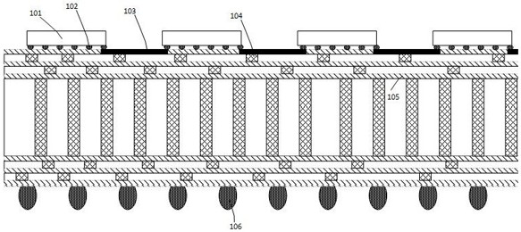
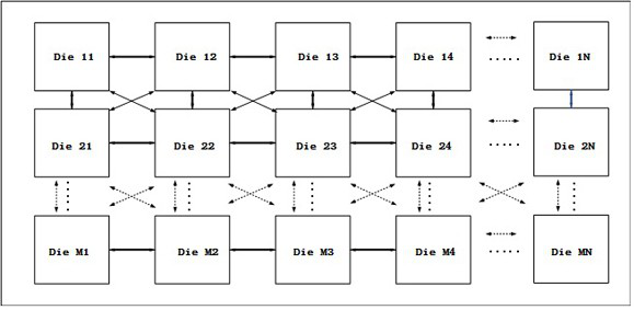
[0023] combine Figure 1-Figure 2 , the present invention describes in detail a low-cost multi-chip high-speed and high-bandwidth interconnection structure suitable for artificial intelligence system integration, including multiple active chips, low-cost interconnection substrates and flip-chip interconnection bumps. The schematic diagram of its structure is as follows figure 1 As shown, the top view is as ...


PUM


Abstract

The invention discloses a low-cost multi-chip high-speed high-bandwidth interconnection structure. The low-cost multi-chip high-speed high-bandwidth interconnection structure comprises a plurality ofactive chips, an interconnection substrate and flip-chip interconnection bumps, wherein the interconnection substrate is used for realizing metal interconnection and mechanical support among the active chips; data exchange between the active chips is achieved through an ultra-high-speed interface, and the active chips jointly bear artificial intelligence computing power; and the active chips are connected with the interconnection substrate in a flip-chip bonding manner through the flip-chip interconnection bumps. The computing power of the artificial intelligence system can be greatly improved, and the manufacturing cost of the artificial intelligence system can be greatly reduced.

Description

technical field [0001] The invention discloses a low-cost multi-chip high-speed and high-bandwidth interconnection structure, and relates to the technical field of system-level integration of artificial intelligence modules. Background technique [0002] Artificial Intelligence (AI), abbreviated as AI, is a science and technology that researches and develops theories, methods, technologies and applications for simulating, extending and expanding human intelligence. With the continuous development of artificial intelligence technology in the fields of machine learning, high-performance computing, image recognition, genetic engineering, etc., the amount of data that artificial intelligence technology needs to process is growing explosively. In an AI training application, the bandwidth requirement of a single SoC may exceed several TB / s. Traditional chip and system integration methods can no longer meet the needs of artificial intelligence technology. At present, Silicon Inte...

Claims


Application Information

Patent Timeline
Patent Type & Authority Applications(China)
IPC IPC(8): H01L23/498H01L23/52H01L23/528H01L23/535H01L23/538
CPCH01L23/49816H01L23/49838H01L23/49844H01L23/52H01L23/5283H01L23/535H01L23/5386
Inventor 谢慧琴李力游蔡宗宇小约翰·罗伯特·罗兰陈希恒韦红芳
Owner 南京蓝洋智能科技有限公司
Features
  • R&D
  • Intellectual Property
  • Life Sciences
  • Materials
  • Tech Scout
  • Unparalleled Data Quality
  • Higher Quality Content
  • 60% Fewer Hallucinations
Learn More