Stacked Cache system based on SEDRAM, control method and Cache device
A stacking and controller technology, applied in the field of stacking cache systems and cache devices, can solve the problems of large cache capacity, large SRAM volume and high price
- Summary
- Abstract
- Description
- Claims
- Application Information
AI Technical Summary
Problems solved by technology
Method used
Image
Examples
Embodiment 1
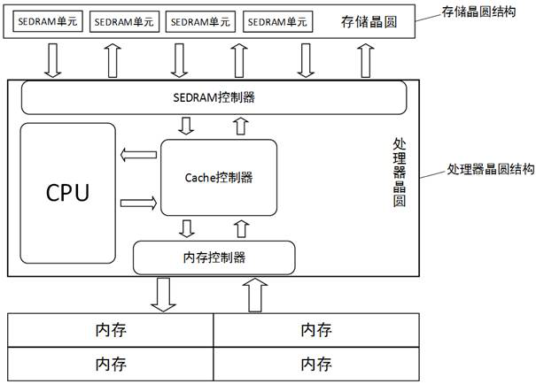
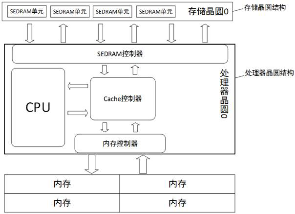
[0075] refer to figure 1 , image 3 , this embodiment provides a stacked Cache system based on SEDRAM, the stacked Cache system is integrated in a multi-layer bonded wafer, and includes a cache memory (Cache), a Cache controller, and a SEDRAM controller; the SEDRAM controller can It can be single-channel or multi-channel parallel access; according to the number of SEDRAM banks, there can be one or more SEDRAM controllers;
[0076] The multilayer bonded wafer includes a storage wafer structure and a processor wafer structure, the storage wafer structure includes at least one layer of storage wafer, and the processor wafer structure includes at least one layer of processor wafer; that is: multilayer bonding A wafer can include a processor wafer and a storage wafer, a multi-layer bonded wafer can also include a processor wafer and two storage wafers, and a multi-layer bonded wafer can also include two layers The processor wafer and one layer of storage wafer, the specific numbe...
Embodiment 2
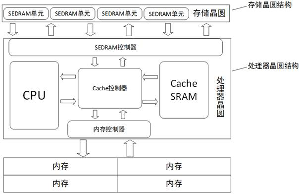
[0083] refer to figure 2 , Figure 4 , this embodiment provides a stacked Cache system based on SEDRAM, the stacked Cache system is integrated in a multi-layer bonded wafer, and includes a cache memory (Cache), a Cache controller, and a SEDRAM controller; the SEDRAM controller can It can be single-channel or multi-channel parallel access; according to the number of SEDRAM banks, there can be one or more SEDRAM controllers;
[0084] The multilayer bonded wafer includes a storage wafer structure and a processor wafer structure, the storage wafer structure includes at least one layer of storage wafer, and the processor wafer structure includes at least one layer of processor wafer; that is: multilayer bonding A wafer can include a processor wafer and a storage wafer, a multi-layer bonded wafer can also include a processor wafer and two storage wafers, and a multi-layer bonded wafer can also include two layers The processor wafer and one layer of storage wafer, the specific num...
Embodiment 3
[0093] refer to Figure 5 , this embodiment provides a Cache control method for any stacked Cache system in the above embodiments, using the SEDRAM unit integrated in each layer of the storage wafer in the storage wafer structure as the Cache system The overall storage space of the Cache is controlled, and both the control domain and the Cache data domain are stored in the SEDRAM unit;
[0094] The concrete steps of this Cache control method are as follows:
[0095] First step S10: the CPU integrated in the processor wafer structure outputs a memory access address;
[0096] Second step S11: According to the memory access address, the Cache controller sends a read request to the SEDRAM controller integrated in the processor wafer structure, and the SEDRAM controller reads the required Cache Line from the SEDRAM unit. The Cache Line includes the control domain and Cache data domain (Cache Data), control domain includes Cache state domain (Cache State) and Cache tag domain (Cac...
PUM
 Abstract
Description
Claims
Application Information


