Method and system for data interaction between cpu and fpga suitable for narrowband channel unit
A narrowband channel and data interaction technology, applied in the direction of electrical digital data processing, advanced technology, instruments, etc., can solve the problems that cannot meet the narrowband channel communication system, redundancy, etc., to save transmission bandwidth, ensure real-time performance, and improve reliability Sexual Transmission Effects
- Summary
- Abstract
- Description
- Claims
- Application Information
AI Technical Summary
Problems solved by technology
Method used
Image
Examples
Embodiment 1
[0055] The invention provides a method for data interaction between CPU and FPGA. The method is suitable for a narrowband channel unit of a communication control device. The method includes the following steps:
[0056] Step 1: On the CPU side, use the SPI interface of the CPU to configure the data transmission and reception on the processor side through the underlying driver, and set the SPI interface on the CPU side as the master side;
[0057] Step 2: On the FPGA side, complete data transmission and reception by writing the SPI interface module, and set the SPI interface on the FPGA side as the slave side;
[0058] Step 3: formulate the SPI data packet protocol, the data interaction is in data packets, the master sends the data packets actively, and the slave sends the data packets by interrupting;
[0059] Step 4: formulate the channel processing flow, according to the narrowband channel type, to ensure the real-time performance of the voice and the reliability of the data...
Embodiment 2
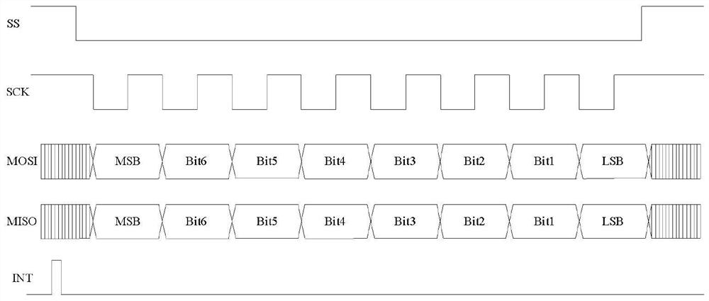
[0074] The CPU model used in the implementation of this example is Loongson 1B, and the FPGA model is Huawei HWD2V6000. The actual connection diagram is as follows figure 1 As shown, connect the four pin lines of the SPI interface of the Loongson 1B processor to the four common IO pins of the FPGA, where ss is the chip select pin, sck is the clock pin, and mosi is the master output and slave input. Data pin, miso is the master input and slave output data pin; in addition, connect an external interrupt pin of Loongson 1B to an ordinary IO pin of FPGA.
Embodiment approach
[0075] figure 2 An implementation method of the present invention is shown, and the method specifically includes the following steps:
[0076] step 1:
[0077] Configure the SPI interface of Loongson 1B. According to the content of Loongson 1B manual, set the d4 of the SPCR register to 1, so that the SPI interface is set as the master; configure the d3 and d2 bits of the SPCR register to 11, so that the clock polarity and phase of the SPI interface are set to cpol=1, cpha =1 mode; configure the d1 and d0 bits of the SPCR register and the d1 and d0 bits of the SPER register as 00 and 01, and set the frequency division factor of the SPI interface to 8, because the source clock of frequency division is half of DDR_CLK (125Mhz) , the clock frequency sck of the SPI in the example is 15.625Mhz.
[0078] Configure the external interrupt of Loongson 1B. According to the content of the Loongson 1B manual, set the external interrupt enable used to be valid, and set the interrupt tr...
PUM
 Abstract
Description
Claims
Application Information


