Planar packaging piece and production method thereof

A package and planar technology, which is applied in the field of planar packages and its production, can solve problems such as failure of bonding wire reliability, lack of improvement in overall package reliability, poor integration, etc., and achieve simplification and reduction of external PCB wiring design The risk of carrier delamination, avoiding the effects of interlaced wires and dense wire bonding

Active Publication Date: 2021-03-26
TIANSHUI 749 ELECTRONICS
View PDF4 Cites 1 Cited by
  • Summary
  • Abstract
  • Description
  • Claims
  • Application Information

AI Technical Summary

Problems solved by technology

When the LQFP planar package has multiple external pins connected to the same potential, all the corresponding internal pins need to be directly connected to the base island, and the welding wires will intersect. Intensive and resulting in reduced reliability issues
[0004] In the existing invention (CN102522392A), a solution to the above-mentioned problem is disclosed by using a grounding ring structure, that is, the ribs passing through the four corners inside the package are connected to the ring island around the base island, and the ring island passes through the base island. The island connection rib is connected to the base island, but because of the high number of LQFP pins, there are often multiple pins that must be wired on the base island to complete the lead-out of the chip substrate potential
This makes the area around the chip must be increased, and in order to avoid being affected by the glue, this makes the area of ​​the base island must be increased, and in order to wire, the base island must be plated with silver, but the combination of silver and plastic packaging materials is very poor, so It will lead to a great increase in the probability of delamination. When a common lead frame has a large number of bonding wires on the base island, there will be intersecting wires or dense bonding, which will affect the electrical performance, and the delamination will cause the reliability and failure of the bonding wires. huge potential risk
[0005] In addition, although the existing LQFP package has a ring-shaped grounding ring, in order to avoid wiring on the base island, the connecting ribs at the four corners inside the package are connected to the ring island around the base island, and the ground wire can be directly connected to the base island. On the ground ring, however, the LQFP package often has multiple pins connected to the same potential. At this time, the wiring of the existing LQFP package is still numerous and scattered, which does not improve the reliability of the overall package. effect

Method used


Image

  • Planar packaging piece and production method thereof
  • Planar packaging piece and production method thereof
  • Planar packaging piece and production method thereof

Examples


Embodiment Construction

[0038] The present invention will be described in detail below with reference to the accompanying drawings and examples. It should be noted that, in the case of no conflict, the embodiments in the present application and the features in the embodiments can be combined with each other.

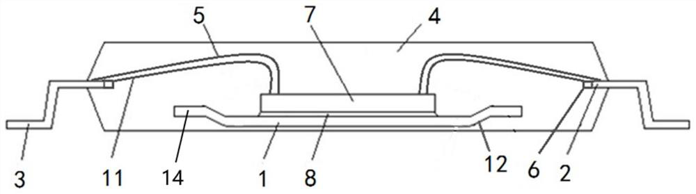
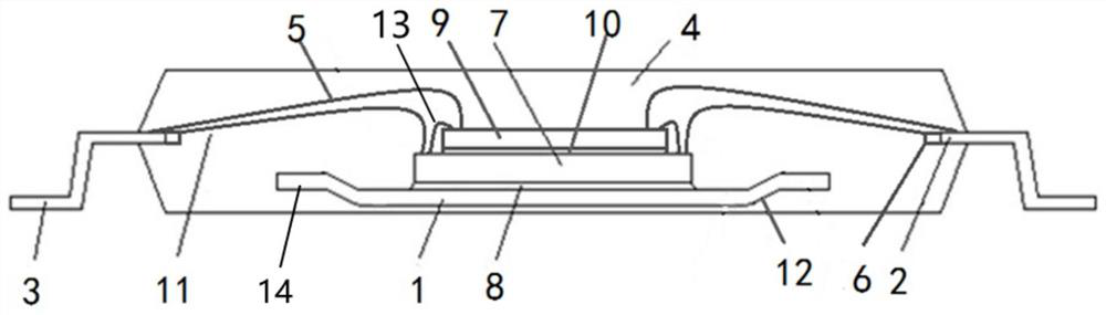
[0039] The following detailed descriptions are all exemplary descriptions, and are intended to provide further detailed descriptions of the present invention. Unless otherwise specified, all technical terms used in the present invention have the same meaning as commonly understood by those of ordinary skill in the art to which the present application belongs. Terms used in the present invention are only for describing specific embodiments, and are not intended to limit exemplary embodiments according to the present invention. The package of the present invention has two forms: single-chip planar package and double-chip planar package. figure 1 is a schematic diagram of the structure of a sing...


PUM


Abstract

The invention provides a planar packaging piece and a production method thereof. The planar packaging piece includes: a base island, a chip pasted on the base island, an inner pin connected with the chip through a welding line, outer pins connected with the inner pin, an interconnection island which is a strip-shaped structure arranged on the inner pin so that the outer pins are interconnected together, and a plastic package body fixedly packaged on the base island, wherein the inner pin, the welding line, the chip and the interconnection island are packaged in the plastic package body, the outer pins are arranged outside the plastic package body, and all the outer pins are positioned on the same plane. According to the invention, a ground wire can be directly arranged between a chip grounding end and the interconnection island, and the ground wire is prevented from being arranged at the edge of the base island. In this way, an external PCB wiring design of the whole packaging piece can be simplified, the base island in the packaging piece is adjusted to the size more matched with the chip, meanwhile, silver does not need to be plated on the base island again (the bonding performance of the contact surface of silver and the plastic packaging material is poor), and a risk of carrier layering is reduced; and routing is performed on the interconnection island so that routing flexibility is improved, and situations of wire crossing and dense routing can be effectively avoided.

Description

technical field [0001] The invention belongs to the technical field of planar packages, in particular to a planar package and a production method thereof. Background technique [0002] At present, electronic products are developing in the direction of multi-function and miniaturization. In this way, high-speed and high-density design requirements are put forward for packaging technology. The SMT (Surface Mounting Technology) packaging technology has been developed, and its representative forms are: PLCC, SOP, SOJ, TSOP, TSSOP, PQFP, QFJ, LQFP and TQFP. Among them, the LQFP (LOW-Profile Quad package) four-side pin flat package is one of the surface mount packages, and the plastic package accounts for the vast majority of the existing packages. It is suitable for small and high-pin thin product packages. The main application Focusing on digital logic circuits such as microprocessors and gate arrays, as well as analog and mixed large-scale integrated circuits, the production p...

Claims


Application Information

Patent Timeline
Patent Type & Authority Applications(China)
IPC IPC(8): H01L23/495H01L23/31H01L21/56H01L21/60
CPCH01L23/4952H01L23/49548H01L23/3114H01L21/56H01L24/83H01L24/85H01L2224/85986H01L2224/83986
Inventor 徐尚军周金成闫景涛郭鹏李习周何文海陈国岚王立国李新平李东何海清王钰中杨保书冯苗陈涛孙伟洪
Owner TIANSHUI 749 ELECTRONICS
Why Eureka
Try Eureka