Learning device, inspection device, learning method, and inspection method

A technology for learning devices and inspection devices, which is applied in measuring devices, machine learning, scientific instruments, etc., can solve the problem of a large number of images, achieve high-precision substrate inspection, and reduce capacity

Pending Publication Date: 2021-04-06
DAINIPPON SCREEN MTG CO LTD
View PDF1 Cites 0 Cited by
  • Summary
  • Abstract
  • Description
  • Claims
  • Application Information

AI Technical Summary

Problems solved by technology

[0004] However, when applying the deep learning technology like Document 1 to the selection of defect images in the inspection device of printed wiring boards, if it is desired to reduce the proportion of false alarms contained in the defect images and improve the inspection accuracy, then There is a concern that the number of images required for learning processing becomes large (that is, the capacity of the learning data set becomes large), and learning takes a lot of time.

Method used


Image

  • Learning device, inspection device, learning method, and inspection method
  • Learning device, inspection device, learning method, and inspection method
  • Learning device, inspection device, learning method, and inspection method

Examples


Embodiment Construction

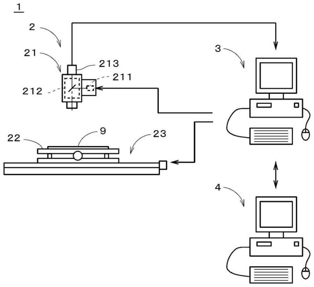
[0043] figure 1 It is a figure which shows the structure of the inspection apparatus 1 which concerns on one Embodiment of this invention. The inspection device 1 is, for example, a device that inspects the appearance of a printed wiring board 9 (hereinafter also simply referred to as "board 9") before mounting electronic components. A pattern (for example, a wiring pattern or an electrode pattern formed of copper) is formed on the surface of the substrate 9 . On the substrate 9 , for example, there are regions where copper plating is exposed, regions where copper wiring is covered with solder resist as a protective film, and regions where solder resist is directly disposed on the surface of the base material.

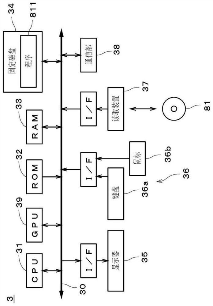
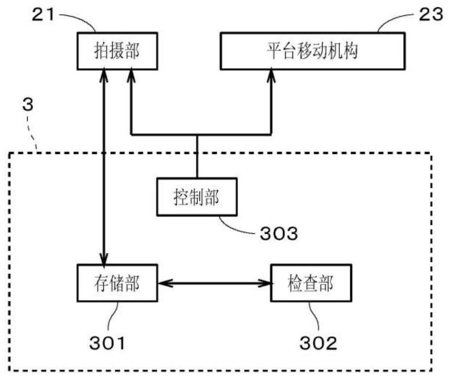
[0044] The inspection apparatus 1 includes: an apparatus body 2 for photographing a substrate 9 , a first computer 3 , and a second computer 4 . The first computer 3 and the second computer 4 are respectively processing devices including a computing unit. The first ...


PUM


Abstract

The invention provides a learning device, an inspection device, a learning method and an inspection method, which can reduce the capacity of a data set for learning and realize high-precision substrate inspection. In the learning device, a second input part inputs second data in which an assumed defect image in first data is re-classified in accordance with the presence or absence of a true defect. The learning part generates a learning data set by weighting the assumed defect image in the second data. The learning part learns the relationship between the substrate image and the presence or absence of the defect by machine learning using the learning data set to generate a learning completion model. In the generation of a learning data set by the learning part, when a hypothetical defect image is re-classified as having a true defect, a weighting coefficient selected according to the degree of importance of the true defect among a plurality of weighting coefficients is multiplied by the hypothetical defect image, and then the hypothetical defect image is classified as having a defect. As a result, the capacity of the learning data set is reduced, and high-precision substrate inspection is achieved.

Description

technical field [0001] The invention relates to a learning device, a checking device, a learning method and a checking method. Background technique [0002] Conventionally, in inspection of printed wiring boards, an inspection device inspects images of each region of the printed wiring board, and selects images judged to have defects (hereinafter referred to as “defective images”). And a defect confirmation operation (so-called verification operation) is performed on the selected defect image by an operator. The defects selected by the inspection device include true defects with a high possibility of becoming a problem in quality and false reports with substantially no possibility of causing a problem in quality. A true defect is selected from the defect images selected by the inspection device. [0003] On the other hand, in Japanese Patent No. 6512585 (Document 1), it is proposed to create a learning binary file by deep learning using a lot of quality image data prepared...

Claims


Application Information

Patent Timeline
IPC IPC(8): G06T7/00G06N20/00G06N3/04G01N21/956G01N21/88
CPCG06T7/0004G06N20/00G01N21/8851G01N21/956G06T2207/30168G06T2207/30141G01N2021/8887G01N2021/95638G06N3/045H01L22/12H01L22/30H01L22/20G01N21/9501G01N21/9515G06T2207/30148
Inventor 塩见顺一
Owner DAINIPPON SCREEN MTG CO LTD
Why Eureka
Try Eureka