Eureka AIR delivers breakthrough ideas for toughest innovation challenges, trusted by R&D personnel around the world.

Photodiode

A photodiode and electrode technology, applied in circuits, lasers, electrical components, etc., can solve the problems of low utilization rate of side-incident MPD lasers, and achieve the effect of reducing chip size and improving responsivity.

Pending Publication Date: 2021-04-06
XIAMEN SANAN INTEGRATED CIRCUIT
View PDF8 Cites 0 Cited by
  • Summary
  • Abstract
  • Description
  • Claims
  • Application Information

AI Technical Summary

Problems solved by technology

[0004] The technical problem to be solved by the present invention is to provide a photodiode, which not only solves the problem of low utilization rate of the side-incidence MPD towards the bottom of the laser, but also improves the responsivity of the side-incidence MPD

Method used


Image

  • Photodiode
  • Photodiode
  • Photodiode

Examples


Embodiment 1

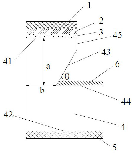
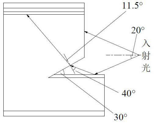
[0030] Embodiment 1: Because the top surface 41, the first incident surface 43 and the mesa 44 indirectly form a zigzag (extend the top surface 41 and the incident surface 43 to intersect), the angle formed by the first incident surface 43 and the mesa 44 θ is 30°, and the divergence angle of the laser is 40° as an example. Since the height a of the mesa 44 will affect the receiving area of ​​light incident, the vertical distance from the mesa 44 to the top surface 41 is ≥ 2 μm. In the first embodiment, taking θ as 30° as an example, the height a of the mesa 44 is 2 μm, and the width of the unopened part of the N-type substrate 4 on the plane where the mesa 44 is located is b, and b>1.77 μm can ensure that light is incident on the photosensitive Layer 3.

[0031] The photodiode of the present invention is used as a side-incidence MPD (MPD is a monitor photodiode, which is a device for monitoring the light output of a laser), and the side-emitting laser is placed next to the si...


PUM

PropertyMeasurementUnit
Thicknessaaaaaaaaaa
Distanceaaaaaaaaaa

Abstract

The present invention discloses a photodiode. The photodiode comprises an N electrode, an N-type substrate, a reflection layer, a photosensitive layer, a P-type layer and a P electrode, the N-type substrate is provided with a top surface, a bottom surface and a side surface for light incidence, the side surface is opened to form a first incident surface and a mesa, and the mesa is lower than the top surface and protrudes out of the top surface, the top surface, the first incident surface and the mesa form a Z shape. The included angle [theta] formed by the first incident plane and the table top is larger than 0 degree and smaller than 90 degrees, the photosensitive layer, the P-type layer and the P electrode are sequentially stacked on the top face, the reflecting layer is stacked on the table top, and the N electrode covers the bottom face. According to the invention, the problem of low utilization rate of laser facing the bottom of the side incidence MPD is solved, and the responsivity of the side incidence MPD is improved.

Description

technical field [0001] The invention relates to the technical field of semiconductor lasers, in particular to a photodiode. Background technique [0002] Backlight Monitor PD, also known as MPD, is an important part of laser components. At present, most of the TO (Transistor Outline, which is a transistor package designed to enable the leads to be molded and used for surface mounting) is in the form of a vertical package, and the MPD is a normal incidence structure. Although normal incidence MPD has mature technology and wide application, it also has obvious disadvantages. The vertical packaging form increases the size of the TO, and the MPD requires spacers, which increases the packaging cost. With the continuous development of optical communication technology, miniaturized TO devices and COB packaging have become the mainstream development direction of the market. [0003] In order to solve the problem of vertical packaging, some companies have introduced side-incidence...

Claims


Application Information

Patent Timeline
IPC IPC(8): H01S5/026
CPCH01S5/0264
Inventor 蔡文必陈振峰
Owner XIAMEN SANAN INTEGRATED CIRCUIT
Why Eureka
Eureka Blog
Learn More